- Based around the Texas Instruments floating-point Digital Signal Processor TMS320C31 running at 32 MHz
- 3U high Compact PCI module
- Quad 16-bit, 10 μsec A/D
- Selectable differential or single-ended inputs
- Quad 16-bit D/A converters with buffered outputs
- Eight TTL digital inputs with internal pull-ups
- Eight TTL digital outputs
- External or internal sample gate logic
- Dual RS232 serial ports
- Front panel I/O accessible
- External power supply input option


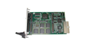
CPCI-ADDA
CPCI 320C31 DSP, 4 channel 16-Bit A/D, 4 Channel 16-bt D/A
- Based around the Texas Instruments floating-point Digital Signal Processor TMS320C31 running at 32 MHz
- 3U high Compact PCI module
- Quad 16-bit, 10 μsec A/D
- Selectable differential or single-ended inputs
- Quad 16-bit D/A converters with buffered outputs
- Eight TTL digital inputs with internal pull-ups
- Eight TTL digital outputs
- External or internal sample gate logic
- Dual RS232 serial ports
- Front panel I/O accessible
- External power supply input option
Share this product
LinkedIn
CPCI-ADDA
CPCI 320C31 DSP, 4 channel 16-Bit A/D, 4 Channel 16-bt D/A
The floating-point 32-bit, 32 MHz DSP TMS320C31 provides input signal conditioning support. However, it seems there might be a discrepancy in the clock speed and memory specifications mentioned. The TMS320C31 typically operates at frequencies ranging from 25 to 80 MHz, not specifically at 32 MHz as mentioned in your query35. Additionally, the TMS320C31 is generally described as having 2K words of on-chip memory, not 512 Kbytes of SRAM9.
Available Software Drivers and Software Tools:
-
-
- C library DLLs
- Linux drivers
- Windows XP drivers
- VxWorks drivers
- LabView
-
Applications:
The CPCI-ADDA supports P.I.D. loop closure frame rates of up to 4 KHz per channel. The CPCI host can download gain and setpoint changes on the fly. The CPCI host can read back the current values for feedback, error, set-point, and output drive on each channel. The local DSP processor can be used for data processing such as digital filters and FFTs. The DSP can also be used as a waveform generator to drive the 16-bit DAC.
TMS320C31 DSP Features:
-
-
- 32-bit floating point DSP at 32 MHz
- Single-cycle instruction execution
- 2 Kbytes of internal RAM
- DMA internal co-processor for concurrent I/O and CPU operation
- Boot loader program built-in
- 64 x 32 internal cache for data
- 2 built-in timers
- Two integer and floating point multipliers
- Parallel multiply and arithmetic/logical operations on integer or floating-point numbers in a single cycle
- Internal or external trigger support for A/D conversion synchronization tied to DSP operations
- Two 32-bit timers which can also be configured for bit I/O
-
PCI Bus Controller Features:
-
-
- Uses the AMCC S5935 PCI controller
- PCI 2.1 compliant master/slave
- 132 Mbytes/sec transfer rate
- Supports Windows NT service pack 2 & 3
- PCI bus operation DC to 33 MHz
- Four definable pass-through data channels
- Two 32-byte internal FIFOs with DMA
- Four mailbox registers with byte-level status and data strobe/interrupts
- Direct PCI and add-on interrupt pins
- Serial nvRAM interface or byte-wide nonvolatile memory interface
- Performs Big Endian/Little Endian conversion
-
AD976A Specifications:
-
-
- Fast 16-bit ADC
- Successive approximation, switched capacitor architecture
- 200 Ksamples/sec throughput – AD976A
- Single 5 V supply operation
- Input range: ±10 VDC
- 100 mW max power dissipation
- Choice of external or internal 2.5 VDC reference
- High-speed parallel interface
- On-chip clock
-
D/A Specifications:
-
-
- Quad 16-bit D/A
-
Digital I/O Specifications:
-
-
- TTL inputs with internal pull-ups
- TTL outputs
-
85C30 Specifications:
-
-
- 2 serial channels
- Up to 1 Mbps using a 16 MHz clock, synchronous mode
- 5, 6, 7, or 8 bits per character
- 1, 1 1/2, or 2 stop bits
- Odd or even parity
- X1, x16, x32, or x64 clock modes
- Character-oriented synchronous capabilities
- SDLC/HLDC capabilities
- NRZ, NRZI, or FM encoding/decoding
- Each serial channel has an independent baud rate generator
- DPLL for clock recovery
-
Instrumentation Amplifier Specifications:
-
-
- Differential input support
- ±10 VDC input range
- Software programmable gain of 1, 2, 4, or 8
- Over-voltage protection to ±40 VDC
-
Operating Environment:
-
-
- Operating temperature:
- Commercial: 0 to +70 ºC
- Optional: -25 ºC to +80 ºC
- Non-operating: -40 ºC to +85 ºC
- Airflow requirement – 5 CFM
- Humidity – 5 to 90% (non-condensing)
- Altitude – 0 to 10,000 feet
- Operating temperature:
-
Mechanical Environment:
-
- Size – 3U CPCI module (100mm x 160mm)
- Single wide PMC 2.92” x 5.87”
- Power – 1.5 watt
- Vibration – 0.5G, 20-2000 Hz random
- Shock – 20G, 11 msec, ½ sine
- Weight – TBD
- MTBF – >250,000 hours
CPCI-ADDA
3U compact PCI with quad 16-bit A/D channels at 100Ksamples/sec and 320C31 DSP
Optional Accessories:
CBL-SCSI-50
50-pin SCSI cable only
TB-50
50-pin terminal block
- Based around the Texas Instruments floating-point Digital Signal Processor TMS320C31 running at 32 MHz
- 3U high Compact PCI module
- Quad 16-bit, 10 μsec A/D
- Selectable differential or single-ended inputs
- Quad 16-bit D/A converters with buffered outputs
- Eight TTL digital inputs with internal pull-ups
- Eight TTL digital outputs
- External or internal sample gate logic
- Dual RS232 serial ports
- Front panel I/O accessible
- External power supply input option
| Mechanical Interface | Switched Mezzanine Card (XMC) Interface confirming to ANSI/VITA 42.0-2008 (Auxiliary Standard) Standard single-width (149mm x 74mm) | |||||||||
| Electrical Interface | PCI Express x4 Link (Base Specification 2.1) compliant interface conforming to ANSI/VITA 42.3-2006 (PCI Express Protocol Layer Standard) | |||||||||
| PCI Express Switch | PI7C9X2G312GP (Pericom) | |||||||||
| PCI Express to PCI Bridge | XIO2001 (Texas Instruments) | |||||||||
| User configurable FPGA | TXMC639-10R: XC7K160T-2FBG676I (AMD) TXMC639-11R: XC7K325T-2FBG676I (AMD) | |||||||||
| SPI-Flash | MT25QL128 (Micron) 128 Mbit (contains TXMC639 FPGA BRD) or compatible; +3.3 V supply voltage | |||||||||
| DDR3 RAM | 2x MT41K256M16TW-107 (Micron) 256Meg x 32 bit | |||||||||
| Board Configuration Controller | LCMXO2-7000HC (Lattice) | |||||||||
| ADC | LTC2320 -16 (Analog Devices) | |||||||||
| DAC | AD5547BRUZ (Analog Devices) | |||||||||
| A/D Channels | TXMC639-10R: 8 Differential 16bit A/D Channels TXMC639-11R: 16 Differential 16bit A/D Channels Input Configuration per BCC Device: Input Voltage Ranges: Differental : ±20.57 V, ±10.28 V or ±5.14 V (Single-Ended: ±10.28 V, ±5.14 V or ±2.57 V) All analog inputs are connected via an impedance converter and a second operation amplifier for level adjustment and filtering to the differential ADC inputs. The -3 dB limit of this input stage is at approx. 8MHz | |||||||||
| D/A Channels | TXMC639-10R: 4 Single-Ended 16 Bit D/A Channels TXMC639-11R: 8 Single-Ended 16 Bit D/A Channels Output range configurable per D/A channel. Maximum single-ended Output Voltage – Vout: ±10 V Maximum Output Drive Current for each Output: 10 mA Maximum Capacitive Load for each Output: 1000 pF Typical Settling Time for a 10 mA / 1000 pF: < 1 µs | |||||||||
| Digital Front I/O Channels | 32 digital I/O Lines
| |||||||||
| Digital Rear I/O Channels | 64 direct FPGA I/O lines to P14 Rear I/O connector
4 MGT line to P16 Rear I/O connector
| |||||||||
| Front I/O | Front I/O Samtec – ERF8_050_01_L_D_RA_L_TR | |||||||||
| P14 Rear I/O | 64 pin Mezzanine Connector (Molex 71436-2864 or compatible) | |||||||||
| P16 Rear I/O | 114 pin Mezzanine Connector (Samtec – ASP-105885-01) | |||||||||
| Power Requirements 1) | Depends on FPGA design With TXMC639 Board Reference Design / without external load
| |||||||||
| Temperature Range | Operating: – 40 °C to + 85 °C Storage: – 55 °C to + 125 °C | |||||||||
| MTBF 1) | 157 000 h to 161 000 h | |||||||||
| Humidity | 5% – 95% non-condensing | |||||||||
| Weight | 140 g |
1) depends on variant, for further details see User Manual
TXMC639-10R
| 8x Analog In, 4x Analog Out, XC7K160T-2FBG676 Kintex™ 7 FPGA AMD Kintex™ 7 FPGA (XC7K160T-2FBG676), 1GB DDR3, 8x Analog In, 4x Analog Out, 32x digital Front I/O, 64x direct FPGA Rear I/O Lines and 4x MGTs Rear I/O |
TXMC639-11R
| 16x Analog In, 8x Analog Out, XC7K325T-2FBG676 Kintex™ 7 FPGA AMD Kintex™ 7 FPGA (XC7K325T-2FBG676), 1GB DDR3, 16x Analog In, 8x Analog Out, 32x digital Front I/O, 64x direct FPGA Rear I/O Lines and 4x MGTs Rear I/O |
SOFTWARE
Share this product
LinkedIn