- 1 or 2 controllers of dual redundant (A/B channel) 1553 communications
- Programmable bus controller, remote terminal, or monitor terminal modes
- MIL-STD-1553 A and B compliant, Notice 2 RT
- STANAG 3838, McAir A3818, and General Dynamics 16PP303 compatible
- BC/RT/MT mode
- 64K words internal RAM with parity
- Long or short stub support
- Front panel I/O


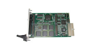
CPCI-1553-DDC
Single or Dual DDC ACE 1553 Controller, BC/RT/MT
- 1 or 2 controllers of dual redundant (A/B channel) 1553 communications
- Programmable bus controller, remote terminal, or monitor terminal modes
- MIL-STD-1553 A and B compliant, Notice 2 RT
- STANAG 3838, McAir A3818, and General Dynamics 16PP303 compatible
- BC/RT/MT mode
- 64K words internal RAM with parity
- Long or short stub support
- Front panel I/O
Share this product
LinkedIn
CPCI-1553-DDC
Single or Dual DDC ACE 1553 Controller, BC/RT/MT
The CPCI-1553-DDC uses Data Device Corporation’s ACE, DDC BU-61865G4-290 communication device as its 1553 bus controller, remote terminal, or monitor terminal. A single controller has two redundant channels, 64Kx16 words of internal memory + parity bit, and internal transceivers for both channels A and B. The 3U compact PCI board has on-board transformers for both channels and controllers and a PCI compliant interface.
Core Component:
- Data Device Corporation’s ACE (DDC BU-61865G4-290)
Functionality:
- Bus Controller, Remote Terminal, or Monitor Terminal
Redundancy:
- Two Redundant Channels (A and B)
Memory:
- 64Kx16 words internal memory + parity
Hardware:
- On-board transformers
Form Factor:
- 3U Compact PCI
Software Support:
- C library DLLs, Linux drivers, Windows XP drivers, VxWorks drivers
Applications:
- Test equipment (evaluation, simulation, monitoring, analysis)
- Operational equipment (avionics, space, aircraft)
- Applications requiring dual terminal functionality
1553 Compliance:
- Data Rate: 1 MHz
- Word Length: 20 bits
- Message Length: Up to 32 data words
- Half-duplex, asynchronous operation
- Manchester II bi-phase encoding
- Command/response protocol
Environmental:
- Operating Temperature: 0 to +55 °C (Commercial), -25 to +85 °C (Optional)
- Non-Operating Temperature: -40 to +85 °C
- Airflow: 5 CFM
- Humidity: 5 to 90% (non-condensing)
- Altitude: 0 to 10,000 ft
Mechanical:
- Size: 3U cPCI Module, 100mm x 160mm
- Power: 5 Watts
- Vibration: 0.5G, 20-2000 Hz rand
- Shock: 20G, 11ms, 1/2 sine
- MTBF: >250,000 Hours
Ordering Information
CPCI-1553-DDC-1:
MIL-1553, BC/RTM, DDC ACE: Single, dual redundant action RT/MT
CPCI-1553-DDC-2:
MIL-1553, BC/RTM, DDC ACE: Dual, dual redundant, same as above with up to full temperature rating
EngKit-1553:
2 Ts, 2 Terminators, 2-1 meter cables
- 1 or 2 controllers of dual redundant (A/B channel) 1553 communications
- Programmable bus controller, remote terminal, or monitor terminal modes
- MIL-STD-1553 A and B compliant, Notice 2 RT
- STANAG 3838, McAir A3818, and General Dynamics 16PP303 compatible
- BC/RT/MT mode
- 64K words internal RAM with parity
- Long or short stub support
- Front panel I/O
| Mechanical Interface | Switched Mezzanine Card (XMC) Interface confirming to ANSI/VITA 42.0-2008 (Auxiliary Standard) Standard single-width (149mm x 74mm) | |||||||||
| Electrical Interface | PCI Express x4 Link (Base Specification 2.1) compliant interface conforming to ANSI/VITA 42.3-2006 (PCI Express Protocol Layer Standard) | |||||||||
| PCI Express Switch | PI7C9X2G312GP (Pericom) | |||||||||
| PCI Express to PCI Bridge | XIO2001 (Texas Instruments) | |||||||||
| User configurable FPGA | TXMC639-10R: XC7K160T-2FBG676I (AMD) TXMC639-11R: XC7K325T-2FBG676I (AMD) | |||||||||
| SPI-Flash | MT25QL128 (Micron) 128 Mbit (contains TXMC639 FPGA BRD) or compatible; +3.3 V supply voltage | |||||||||
| DDR3 RAM | 2x MT41K256M16TW-107 (Micron) 256Meg x 32 bit | |||||||||
| Board Configuration Controller | LCMXO2-7000HC (Lattice) | |||||||||
| ADC | LTC2320 -16 (Analog Devices) | |||||||||
| DAC | AD5547BRUZ (Analog Devices) | |||||||||
| A/D Channels | TXMC639-10R: 8 Differential 16bit A/D Channels TXMC639-11R: 16 Differential 16bit A/D Channels Input Configuration per BCC Device: Input Voltage Ranges: Differental : ±20.57 V, ±10.28 V or ±5.14 V (Single-Ended: ±10.28 V, ±5.14 V or ±2.57 V) All analog inputs are connected via an impedance converter and a second operation amplifier for level adjustment and filtering to the differential ADC inputs. The -3 dB limit of this input stage is at approx. 8MHz | |||||||||
| D/A Channels | TXMC639-10R: 4 Single-Ended 16 Bit D/A Channels TXMC639-11R: 8 Single-Ended 16 Bit D/A Channels Output range configurable per D/A channel. Maximum single-ended Output Voltage – Vout: ±10 V Maximum Output Drive Current for each Output: 10 mA Maximum Capacitive Load for each Output: 1000 pF Typical Settling Time for a 10 mA / 1000 pF: < 1 µs | |||||||||
| Digital Front I/O Channels | 32 digital I/O Lines
| |||||||||
| Digital Rear I/O Channels | 64 direct FPGA I/O lines to P14 Rear I/O connector
4 MGT line to P16 Rear I/O connector
| |||||||||
| Front I/O | Front I/O Samtec – ERF8_050_01_L_D_RA_L_TR | |||||||||
| P14 Rear I/O | 64 pin Mezzanine Connector (Molex 71436-2864 or compatible) | |||||||||
| P16 Rear I/O | 114 pin Mezzanine Connector (Samtec – ASP-105885-01) | |||||||||
| Power Requirements 1) | Depends on FPGA design With TXMC639 Board Reference Design / without external load
| |||||||||
| Temperature Range | Operating: – 40 °C to + 85 °C Storage: – 55 °C to + 125 °C | |||||||||
| MTBF 1) | 157 000 h to 161 000 h | |||||||||
| Humidity | 5% – 95% non-condensing | |||||||||
| Weight | 140 g |
1) depends on variant, for further details see User Manual
TXMC639-10R
| 8x Analog In, 4x Analog Out, XC7K160T-2FBG676 Kintex™ 7 FPGA AMD Kintex™ 7 FPGA (XC7K160T-2FBG676), 1GB DDR3, 8x Analog In, 4x Analog Out, 32x digital Front I/O, 64x direct FPGA Rear I/O Lines and 4x MGTs Rear I/O |
TXMC639-11R
| 16x Analog In, 8x Analog Out, XC7K325T-2FBG676 Kintex™ 7 FPGA AMD Kintex™ 7 FPGA (XC7K325T-2FBG676), 1GB DDR3, 16x Analog In, 8x Analog Out, 32x digital Front I/O, 64x direct FPGA Rear I/O Lines and 4x MGTs Rear I/O |
SOFTWARE
Share this product
LinkedIn