- Based on FPGA Logic I/O controllers
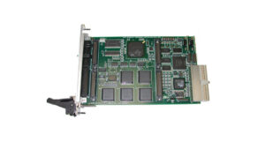
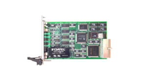
- CompactPCI 3U module
- Front panel I/O
- 48 outputs optically isolated
- Isolated up to 2500V
- Open collector outputs with 100 mA continuous current sink support
- Pin Programmable with Read back feature
- 0 -30V operation range
- Up to 70V overvoltage protection provided
- Less than 100 µs opto isolator
- MTBF <200000
CPCI-48 OUT
CPCI 48 Optically Isolated Outputs Card
- Based on FPGA Logic I/O controllers
- CompactPCI 3U module
- Front panel I/O
- 48 outputs optically isolated
- Isolated up to 2500V
- Open collector outputs with 100 mA continuous current sink support
- Pin Programmable with Read back feature
- 0 -30V operation range
- Up to 70V overvoltage protection provided
- Less than 100 µs opto isolator
- MTBF <200000
Share this product
LinkedIn
The output board, designed for DC output control, utilizes FPGA controllers to ensure precise timing. Each output channel incorporates optical isolation and supports an open collector configuration. A PCI controller provides seamless integration with the host computer, and all input/output connections are conveniently located on the front panel.
Available Software Drivers and Software Tools:
-
-
- C library DLLs
- Windows and Linux drivers available
-
Applications:
The CPCI-48OUT is the complement to the CPCI-48IN. The CPCI-48OUT offers 48 channels of optically isolated output connections.
FPGA Features:
-
-
- Two independent 8-bit, double-buffered bidirectional I/O ports
- I/O ports feature programmable polarity
- Programmable direction at the bit level
- Flexible pattern-recognition logic; programmable as a 16-bit vector interrupt controller
- Three independent 16-bit counter/timers with up to four external access lines per counter/timer
- Four handshake modes
- All internal registers are readable and writable
- All registers have their own unique address so that they can be accessed directly
-
PCI Bus Controller Features:
-
-
- PLX 9056 33/66MHz 32-bit, PCI r2.2 compliant
- Motorola PowerQUICC and generic 32-bit, 66MHz local bus modes
- 3.3V I/O, 5V tolerant bus interfaces
- PICMG 2.1 r2.0 hot swap
- Zero wait state burst operation, with PCI bus bursts to 264 MB/sec and local bus bursts to 264 MB/sec
- 2 DMA channels
- Direct master data transfers
- Direct slave data transfers
-
I/O Specifications:
-
-
- 48 output pins, front panel accessible
- SCSI-style front panel connector
- Output supports continuous 100 mA DC load
- Optically isolated to 2500 VDC
- Output saturation of +0.3 VDC under 100 mA load
-
Operating Environment:
-
-
- Operating temperature:
- Commercial: 0 to +70 ºC
- Optional: -40 ºC to +80 ºC
- Non-operating: -55 ºC to +95 ºC
- Airflow requirement – 5 CFM
- Humidity – 5 to 90% (non-condensing)
- Altitude – 0 to 10,000 feet
- Operating temperature:
-
Mechanical Environment:
-
- Size – 3U CPCI module (100mm x 160mm)
- Vibration – 0.5G, 20-2000 Hz random
- Shock – 20G, 11 msec, ½ sine
- Weight – 4 ounces
- MTBF – >250,000 hours
The CPCI-48OUT:
48 channel output: optically isolated
Optional accessories:
- TB-100: Terminal block and cable.
- CBL-100: 100 pin cable only.
- Based on FPGA Logic I/O controllers
- CompactPCI 3U module
- Front panel I/O
- 48 outputs optically isolated
- Isolated up to 2500V
- Open collector outputs with 100 mA continuous current sink support
- Pin Programmable with Read back feature
- 0 -30V operation range
- Up to 70V overvoltage protection provided
- Less than 100 µs opto isolator
- MTBF <200000
| Mechanical Interface | Switched Mezzanine Card (XMC) Interface confirming to ANSI/VITA 42.0-2008 (Auxiliary Standard) Standard single-width (149mm x 74mm) | |||||||||
| Electrical Interface | PCI Express x4 Link (Base Specification 2.1) compliant interface conforming to ANSI/VITA 42.3-2006 (PCI Express Protocol Layer Standard) | |||||||||
| PCI Express Switch | PI7C9X2G312GP (Pericom) | |||||||||
| PCI Express to PCI Bridge | XIO2001 (Texas Instruments) | |||||||||
| User configurable FPGA | TXMC639-10R: XC7K160T-2FBG676I (AMD) TXMC639-11R: XC7K325T-2FBG676I (AMD) | |||||||||
| SPI-Flash | MT25QL128 (Micron) 128 Mbit (contains TXMC639 FPGA BRD) or compatible; +3.3 V supply voltage | |||||||||
| DDR3 RAM | 2x MT41K256M16TW-107 (Micron) 256Meg x 32 bit | |||||||||
| Board Configuration Controller | LCMXO2-7000HC (Lattice) | |||||||||
| ADC | LTC2320 -16 (Analog Devices) | |||||||||
| DAC | AD5547BRUZ (Analog Devices) | |||||||||
| A/D Channels | TXMC639-10R: 8 Differential 16bit A/D Channels TXMC639-11R: 16 Differential 16bit A/D Channels Input Configuration per BCC Device: Input Voltage Ranges: Differental : ±20.57 V, ±10.28 V or ±5.14 V (Single-Ended: ±10.28 V, ±5.14 V or ±2.57 V) All analog inputs are connected via an impedance converter and a second operation amplifier for level adjustment and filtering to the differential ADC inputs. The -3 dB limit of this input stage is at approx. 8MHz | |||||||||
| D/A Channels | TXMC639-10R: 4 Single-Ended 16 Bit D/A Channels TXMC639-11R: 8 Single-Ended 16 Bit D/A Channels Output range configurable per D/A channel. Maximum single-ended Output Voltage – Vout: ±10 V Maximum Output Drive Current for each Output: 10 mA Maximum Capacitive Load for each Output: 1000 pF Typical Settling Time for a 10 mA / 1000 pF: < 1 µs | |||||||||
| Digital Front I/O Channels | 32 digital I/O Lines
| |||||||||
| Digital Rear I/O Channels | 64 direct FPGA I/O lines to P14 Rear I/O connector
4 MGT line to P16 Rear I/O connector
| |||||||||
| Front I/O | Front I/O Samtec – ERF8_050_01_L_D_RA_L_TR | |||||||||
| P14 Rear I/O | 64 pin Mezzanine Connector (Molex 71436-2864 or compatible) | |||||||||
| P16 Rear I/O | 114 pin Mezzanine Connector (Samtec – ASP-105885-01) | |||||||||
| Power Requirements 1) | Depends on FPGA design With TXMC639 Board Reference Design / without external load
| |||||||||
| Temperature Range | Operating: – 40 °C to + 85 °C Storage: – 55 °C to + 125 °C | |||||||||
| MTBF 1) | 157 000 h to 161 000 h | |||||||||
| Humidity | 5% – 95% non-condensing | |||||||||
| Weight | 140 g |
1) depends on variant, for further details see User Manual
TXMC639-10R
| 8x Analog In, 4x Analog Out, XC7K160T-2FBG676 Kintex™ 7 FPGA AMD Kintex™ 7 FPGA (XC7K160T-2FBG676), 1GB DDR3, 8x Analog In, 4x Analog Out, 32x digital Front I/O, 64x direct FPGA Rear I/O Lines and 4x MGTs Rear I/O |
TXMC639-11R
| 16x Analog In, 8x Analog Out, XC7K325T-2FBG676 Kintex™ 7 FPGA AMD Kintex™ 7 FPGA (XC7K325T-2FBG676), 1GB DDR3, 16x Analog In, 8x Analog Out, 32x digital Front I/O, 64x direct FPGA Rear I/O Lines and 4x MGTs Rear I/O |
SOFTWARE
Share this product
LinkedIn