- Based around the Texas Instruments floating-point Digital Signal Processor TMS320C32 at 60 MHz
- 3U high Compact PCI module
- 8 16-bit channels with optional 8 additional channels on mezzanine
- 100 Ks/sec or optional 200 Ks/sec A/D
- 8Kword sample buffer FIFO
- External or internal or PXI sample gate logic
- Differential instrumentation amplifier for each analog input
- Programmable gain 1, 2, 4, 8 standard; 1, 10, 100, 1000 optional
- External power supply input option
- PXI support with front panel I/O


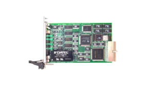
CPCI-AD8
CPCI-AD8 DSP C32, 8/16 Channel 16-Bit A/D
- Based around the Texas Instruments floating-point Digital Signal Processor TMS320C32 at 60 MHz
- 3U high Compact PCI module
- 8 16-bit channels with optional 8 additional channels on mezzanine
- 100 Ks/sec or optional 200 Ks/sec A/D
- 8Kword sample buffer FIFO
- External or internal or PXI sample gate logic
- Differential instrumentation amplifier for each analog input
- Programmable gain 1, 2, 4, 8 standard; 1, 10, 100, 1000 optional
- External power supply input option
- PXI support with front panel I/O
Share this product
LinkedIn
CPCI-AD8
CPCI-AD8 DSP C32, 8/16 Channel 16-Bit A/D
The floating-point 32-bit, 60 MHz DSP TMS320C32 provides input signal conditioning support and is backed by 512 Kbytes of zero wait state SRAM for temporary storage and DSP operations, along with 4 Mbits of flash. Eight input instrumentation amplifiers ensure differential input buffering and gain, while A/D operations can be triggered internally or externally via the front panel. An 8K-word FIFO enables sample buffering, and a PCIbus connector facilitates the interface to the host computer. Additionally, this module can utilize an external power source for reduced noise operation.
Available Software Drivers and Software Tools:
-
-
- C library dll’s
- Linux drivers
- Windows XP drivers
- VxWorks drivers
- LabView
-
Applications: The Local DSP can be used to simply move data to and from the CPCI bus or provide pre-processing functions such as limit checking, FFTs, digital filtering, etc. Custom application software can be downloaded to the DSP via the CompactPCI bus.
TMS320C32 DSP Features:
-
-
- 32/40-bit floating point DSP at 60 MHz
- 60 million floating-point operations (MFLOPS)
- Two 256 x 32-bit single-cycle, dual-access on-chip RAM blocks
- One serial port
- Two 32-bit timers
- Two DMA internal co-processors
- Boot loader program built-in
- 64 x 32-bit on-board program cache
- Internal or external trigger support for A/D conversion synchronization tied to DSP operations
-
AD976A Specifications:
-
-
- Fast 16-bit ADC
- Successive approximation, switched capacitor architecture
- 200 Ksamples/sec throughput – AD976A
- Single 5 V supply operation
- Input range: ±10 VDC
- 100 mW max power dissipation
- Choice of external or internal 2.5 VDC reference
- High-speed parallel interface
- On-chip clock
-
Instrumentation Amplifier Specifications:
-
-
- Differential input support
- ±10VDC input range
- Software programmable gain of 1, 2, 4, or 8; optional 1, 10, 100, 1000
- Over-voltage protection to ±40 VDC
-
Operating Environment:
-
-
- Operating temperature: Commercial: 0 to +70 ºC, Optional: -25 ºC to +80 ºC
- Non-operating temperature: -40 ºC to +85 ºC
- Airflow requirement – 5 CFM
- Humidity – 5 to 90% (non-condensing)
- Altitude – 0 to 10,000 feet
-
PCI Bus Controller Features:
-
-
- The PLX PCI 9080 is PCI Version 2.1 compliant
- Bus Master interface chip for adapters and embedded systems
- Programmable local bus supports non-multiplexed 32-bit address/data, multiplexed 32- or 16-bit, and accesses of 32-, 16-, or 8-bit local bus devices
- I2O compatible messaging unit
- 3.3 or 5 volt PCI signaling, 5 volt core, low-power CMOS in 208-pin PQFP
- Two independent programmable DMA channels for local bus memory to/from PCI host bus data transfers
- Eight programmable FIFOs for zero wait state burst operation
- PCI to/from local data transfers up to 133MB/sec
- Local bus runs asynchronously to the PCI bus
- Eight 32-bit mailbox and two 32-bit doorbell registers
- Performs Big Endian/Little Endian conversion
-
Mechanical Environment:
-
- Size – 3U CPCI module (100mm x 160mm)
- Power – 1.5 watt
- Vibration – 0.5G, 20-2000 Hz random
- Shock – 20G, 11 msec, ½ sine
- Weight – 3 ounces
- MTBF – >250,000 hours
CPCI-AD8:
3U compact PCI with 8 16-bit A/D channels at 100K samples/sec and a 320C32 DSP
Option-200:
w/200K samples/sec A/D channels
Option-16:
8 additional channels of 16-bit A/D on mezzanine
Optional Accessories
TB-50:
50-pin terminal block with cable
CBL-SCSI-50:
50-pin SCSI to SCSI cable only
- Based around the Texas Instruments floating-point Digital Signal Processor TMS320C32 at 60 MHz
- 3U high Compact PCI module
- 8 16-bit channels with optional 8 additional channels on mezzanine
- 100 Ks/sec or optional 200 Ks/sec A/D
- 8Kword sample buffer FIFO
- External or internal or PXI sample gate logic
- Differential instrumentation amplifier for each analog input
- Programmable gain 1, 2, 4, 8 standard; 1, 10, 100, 1000 optional
- External power supply input option
- PXI support with front panel I/O
| Mechanical Interface | Switched Mezzanine Card (XMC) Interface confirming to ANSI/VITA 42.0-2008 (Auxiliary Standard) Standard single-width (149mm x 74mm) | |||||||||
| Electrical Interface | PCI Express x4 Link (Base Specification 2.1) compliant interface conforming to ANSI/VITA 42.3-2006 (PCI Express Protocol Layer Standard) | |||||||||
| PCI Express Switch | PI7C9X2G312GP (Pericom) | |||||||||
| PCI Express to PCI Bridge | XIO2001 (Texas Instruments) | |||||||||
| User configurable FPGA | TXMC639-10R: XC7K160T-2FBG676I (AMD) TXMC639-11R: XC7K325T-2FBG676I (AMD) | |||||||||
| SPI-Flash | MT25QL128 (Micron) 128 Mbit (contains TXMC639 FPGA BRD) or compatible; +3.3 V supply voltage | |||||||||
| DDR3 RAM | 2x MT41K256M16TW-107 (Micron) 256Meg x 32 bit | |||||||||
| Board Configuration Controller | LCMXO2-7000HC (Lattice) | |||||||||
| ADC | LTC2320 -16 (Analog Devices) | |||||||||
| DAC | AD5547BRUZ (Analog Devices) | |||||||||
| A/D Channels | TXMC639-10R: 8 Differential 16bit A/D Channels TXMC639-11R: 16 Differential 16bit A/D Channels Input Configuration per BCC Device: Input Voltage Ranges: Differental : ±20.57 V, ±10.28 V or ±5.14 V (Single-Ended: ±10.28 V, ±5.14 V or ±2.57 V) All analog inputs are connected via an impedance converter and a second operation amplifier for level adjustment and filtering to the differential ADC inputs. The -3 dB limit of this input stage is at approx. 8MHz | |||||||||
| D/A Channels | TXMC639-10R: 4 Single-Ended 16 Bit D/A Channels TXMC639-11R: 8 Single-Ended 16 Bit D/A Channels Output range configurable per D/A channel. Maximum single-ended Output Voltage – Vout: ±10 V Maximum Output Drive Current for each Output: 10 mA Maximum Capacitive Load for each Output: 1000 pF Typical Settling Time for a 10 mA / 1000 pF: < 1 µs | |||||||||
| Digital Front I/O Channels | 32 digital I/O Lines
| |||||||||
| Digital Rear I/O Channels | 64 direct FPGA I/O lines to P14 Rear I/O connector
4 MGT line to P16 Rear I/O connector
| |||||||||
| Front I/O | Front I/O Samtec – ERF8_050_01_L_D_RA_L_TR | |||||||||
| P14 Rear I/O | 64 pin Mezzanine Connector (Molex 71436-2864 or compatible) | |||||||||
| P16 Rear I/O | 114 pin Mezzanine Connector (Samtec – ASP-105885-01) | |||||||||
| Power Requirements 1) | Depends on FPGA design With TXMC639 Board Reference Design / without external load
| |||||||||
| Temperature Range | Operating: – 40 °C to + 85 °C Storage: – 55 °C to + 125 °C | |||||||||
| MTBF 1) | 157 000 h to 161 000 h | |||||||||
| Humidity | 5% – 95% non-condensing | |||||||||
| Weight | 140 g |
1) depends on variant, for further details see User Manual
TXMC639-10R
| 8x Analog In, 4x Analog Out, XC7K160T-2FBG676 Kintex™ 7 FPGA AMD Kintex™ 7 FPGA (XC7K160T-2FBG676), 1GB DDR3, 8x Analog In, 4x Analog Out, 32x digital Front I/O, 64x direct FPGA Rear I/O Lines and 4x MGTs Rear I/O |
TXMC639-11R
| 16x Analog In, 8x Analog Out, XC7K325T-2FBG676 Kintex™ 7 FPGA AMD Kintex™ 7 FPGA (XC7K325T-2FBG676), 1GB DDR3, 16x Analog In, 8x Analog Out, 32x digital Front I/O, 64x direct FPGA Rear I/O Lines and 4x MGTs Rear I/O |
SOFTWARE
Share this product
LinkedIn