- 1 or 2 controllers of dual redundant (A/B channel) 1553 communications
- Programmable bus controller, remote terminal, or monitor terminal modes
- MIL-STD-1553 A and B compliant, Notice 2 RT
- Long or short stub support
- Low power consumption
- Front I/O panel
- On-chip transceivers
- PICMG compliant
- Single +5 VDC supply
- Simultaneous RT/M mode
- Remote terminal address input

CPCI-1553-UTMC
Single or Dual UTMC LXE/DXE 1553 Controller
- 1 or 2 controllers of dual redundant (A/B channel) 1553 communications
- Programmable bus controller, remote terminal, or monitor terminal modes
- MIL-STD-1553 A and B compliant, Notice 2 RT
- Long or short stub support
- Low power consumption
- Front I/O panel
- On-chip transceivers
- PICMG compliant
- Single +5 VDC supply
- Simultaneous RT/M mode
- Remote terminal address input
Share this product
LinkedIn
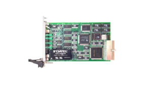
CPCI-1553-UTMC
Single or Dual UTMC LXE/DXE 1553 Controller
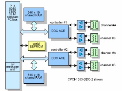
The CPCI-1553-UTMC-1,2 uses UTMC’s Sμmmit LXE/DXE version, UT69151DXE-GPC 1553 communication device as its 1553 bus controller, or remote terminal, or monitor terminal. A single controller has two redundant channels and built-in transceivers. The 1553 board can have 1 or 2 communication channels. The controller accesses 64Kx16 words of external memory and has internal transceivers for both channel A and B. The 3U CPCI board has on-board transformers for both channels and both controllers. The board format is a compact PCI board layout.
Available Software Drivers:
- C library DLLs
- Linux drivers
- Windows XP drivers
- VxWorks drivers
Applications:
This is a perfect solution for a wide array of 1553 communication applications, such as:
- Test equipment supporting evaluation, simulation, monitoring, and analysis
- Operational equipment like avionics, space satellite systems, aircraft onboard systems, commercial systems, etc.
- Applications that require dual functionality of the terminal for monitoring and remote operation at the same time
1553 Compliance/Characteristics:
- Data Rate: 1 MHz
- Word Length: 20 bits
- Data Bits/Word: 16 bits
- Message Length: Maximum of 32 data words
- Transmission Technique: Half-duplex
- Operation: Asynchronous
- Transmission Encoding: Manchester II, bi-phase
- Protocol: Command/response
- Bus Control: Single or multiple
- Fault Tolerance: Typically dual redundant, second bus in “hot backup” status
- Message Formats: Controller to terminal, terminal to controller, terminal to terminal, broadcast, system control
- Number of Remote Terminals: Maximum 31
- Terminal Types: Remote terminal, bus controller, bus monitor
- Transmission Media: Twisted shielded pair
- Coupling: Transformer and direct
UTMC/Summit/LXE/DXE Features:
- The UT69151DXE-GPC has integrated transceivers
- RT mode internal command illegalization
- 16-bit read/write time-tag with user-defined resolution
- Sub-address data buffering
- Simultaneous RT/MT mode of operation
- BC architecture designed with:
- Minor frame timing
- Efficient command block flow statements
- Status word polling
- Programmable retries
- Programmable interrupt architecture
- Autonomous operation in all three modes
- Supports IEEE Standard 1149.1 (JTAG)
PCI Bus Controller Features:
- Uses the AMCC S5935 PCI controller
- PCI 2.1 compliant master/slave
- 132 Mbytes/sec transfer rate
- Supports Windows NT service pack 2 & 3
- PCI bus operation DC to 33 MHz
- Four definable pass-through data channels
- Two 32 byte internal FIFOs with DMA
- Four mail box registers with byte level status and data strobe/interrupts
- Direct PCI and add-on interrupt pins
- Serial nvRAM interface or byte-wide non-volatile memory interface
Operating Environment:
- Operating temperature:
- Commercial: 0 to +55°C
- Optional: -25°C to +80°C
- Extended: -40°C to +85°C
- Airflow requirement – 5 CFM
- Humidity – 5 to 90% (non-cond)
- Altitude – 0 to 10,000 feet
- Option: Conformal Coating
Mechanical Environment:
- Size – 3U CPCI module, 100mm x 160mm
- Power – 1.5 watt
- Front panel I/O
- Vibration – 0.5G, 20-2000 Hz random
- Shock – 20G, 11 msec, 1⁄2 sine
- Weight – 4 ounces
- MTBF – >250,000 hours
Terminal Electrical Input Characteristics
| Requirement | Transformer Coupled | Direct Coupled |
|---|---|---|
| Input level | 0.866-14.0V | 1.2-20.0V |
| No response | 0.0-0.2V | 0.0-0.28V |
| Zero crossing stability | +/-150.0 nSec | +/-150.0 nSec |
| Rise/fall times | 0 nsec – Sine | 0 nsec – Sine |
| Noise rejection | 140 mV WGN | 200 mV WGN |
| Common mode rejection | +/- 10.0V peak | +/- 10.0V peak |
| Input impedance | 1000 ohms | 2000 ohms |
Terminal Electrical Output Characteristics
| Requirement | Transformer Coupled | Direct Coupled |
|---|---|---|
| Output level | 18.0-27.0V | 6.0-9.0V |
| Zero crossing stability | 25.0 nsec | 25.0 nsec |
| Rise/fall | 100-300 nsec | 100-300 nsec |
| Max distortion | +/-900.0 mV | +/- 300.0 mV |
| Max output noise | 14.0 mV | 5.0 mV |
| Max residual voltage | +/-250.0 mV | +/-90.0 mV |
- CPCI-1553-1: MIL-1553, BC/RT/M, UTMC Summit; PMC module
- CPCI-1553-2: MIL-1553, BC/RT/M, UTMC Summit; PMC module; 2 controllers
- Option I: Same as above with -40°C to +85°C temperature rating
Optional Accessories
- EngKit-1553: 2 T’s, 2 Terminators, 2-1 meter cables
- CBL-1553-1: Standard-standard 2 meter 1553 cable
- CPL-1553-2: Standard-mini 2 meter 1553 cable
- CBL-1553-3: Mini-mini 2 meter 1553 cable
- 1 or 2 controllers of dual redundant (A/B channel) 1553 communications
- Programmable bus controller, remote terminal, or monitor terminal modes
- MIL-STD-1553 A and B compliant, Notice 2 RT
- Long or short stub support
- Low power consumption
- Front I/O panel
- On-chip transceivers
- PICMG compliant
- Single +5 VDC supply
- Simultaneous RT/M mode
- Remote terminal address input
| Mechanical Interface | Switched Mezzanine Card (XMC) Interface confirming to ANSI/VITA 42.0-2008 (Auxiliary Standard) Standard single-width (149mm x 74mm) | |||||||||
| Electrical Interface | PCI Express x4 Link (Base Specification 2.1) compliant interface conforming to ANSI/VITA 42.3-2006 (PCI Express Protocol Layer Standard) | |||||||||
| PCI Express Switch | PI7C9X2G312GP (Pericom) | |||||||||
| PCI Express to PCI Bridge | XIO2001 (Texas Instruments) | |||||||||
| User configurable FPGA | TXMC639-10R: XC7K160T-2FBG676I (AMD) TXMC639-11R: XC7K325T-2FBG676I (AMD) | |||||||||
| SPI-Flash | MT25QL128 (Micron) 128 Mbit (contains TXMC639 FPGA BRD) or compatible; +3.3 V supply voltage | |||||||||
| DDR3 RAM | 2x MT41K256M16TW-107 (Micron) 256Meg x 32 bit | |||||||||
| Board Configuration Controller | LCMXO2-7000HC (Lattice) | |||||||||
| ADC | LTC2320 -16 (Analog Devices) | |||||||||
| DAC | AD5547BRUZ (Analog Devices) | |||||||||
| A/D Channels | TXMC639-10R: 8 Differential 16bit A/D Channels TXMC639-11R: 16 Differential 16bit A/D Channels Input Configuration per BCC Device: Input Voltage Ranges: Differental : ±20.57 V, ±10.28 V or ±5.14 V (Single-Ended: ±10.28 V, ±5.14 V or ±2.57 V) All analog inputs are connected via an impedance converter and a second operation amplifier for level adjustment and filtering to the differential ADC inputs. The -3 dB limit of this input stage is at approx. 8MHz | |||||||||
| D/A Channels | TXMC639-10R: 4 Single-Ended 16 Bit D/A Channels TXMC639-11R: 8 Single-Ended 16 Bit D/A Channels Output range configurable per D/A channel. Maximum single-ended Output Voltage – Vout: ±10 V Maximum Output Drive Current for each Output: 10 mA Maximum Capacitive Load for each Output: 1000 pF Typical Settling Time for a 10 mA / 1000 pF: < 1 µs | |||||||||
| Digital Front I/O Channels | 32 digital I/O Lines
| |||||||||
| Digital Rear I/O Channels | 64 direct FPGA I/O lines to P14 Rear I/O connector
4 MGT line to P16 Rear I/O connector
| |||||||||
| Front I/O | Front I/O Samtec – ERF8_050_01_L_D_RA_L_TR | |||||||||
| P14 Rear I/O | 64 pin Mezzanine Connector (Molex 71436-2864 or compatible) | |||||||||
| P16 Rear I/O | 114 pin Mezzanine Connector (Samtec – ASP-105885-01) | |||||||||
| Power Requirements 1) | Depends on FPGA design With TXMC639 Board Reference Design / without external load
| |||||||||
| Temperature Range | Operating: – 40 °C to + 85 °C Storage: – 55 °C to + 125 °C | |||||||||
| MTBF 1) | 157 000 h to 161 000 h | |||||||||
| Humidity | 5% – 95% non-condensing | |||||||||
| Weight | 140 g |
1) depends on variant, for further details see User Manual
TXMC639-10R
| 8x Analog In, 4x Analog Out, XC7K160T-2FBG676 Kintex™ 7 FPGA AMD Kintex™ 7 FPGA (XC7K160T-2FBG676), 1GB DDR3, 8x Analog In, 4x Analog Out, 32x digital Front I/O, 64x direct FPGA Rear I/O Lines and 4x MGTs Rear I/O |
TXMC639-11R
| 16x Analog In, 8x Analog Out, XC7K325T-2FBG676 Kintex™ 7 FPGA AMD Kintex™ 7 FPGA (XC7K325T-2FBG676), 1GB DDR3, 16x Analog In, 8x Analog Out, 32x digital Front I/O, 64x direct FPGA Rear I/O Lines and 4x MGTs Rear I/O |
SOFTWARE
Share this product
LinkedIn