- Based around the Texas Instruments floating-point Digital Signal Processor TMS-320C6713
- Dual industry pack carrier configuration enabling a vast array of I/O possibilities, creating a cost-effective solution for DSP and I/O
- Compact PCI bus compatible
- Virtually unlimited customization of the input-output functions as well as hardware-accelerated signal processing
- Adds high-speed, low latency I/O and deterministic control to a low-cost PC system solution


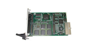
CPCI-6713-2IP
CPCI 320C6317B DSP Dual Industry Pack Carrier
- Based around the Texas Instruments floating-point Digital Signal Processor TMS-320C6713
- Dual industry pack carrier configuration enabling a vast array of I/O possibilities, creating a cost-effective solution for DSP and I/O
- Compact PCI bus compatible
- Virtually unlimited customization of the input-output functions as well as hardware-accelerated signal processing
- Adds high-speed, low latency I/O and deterministic control to a low-cost PC system solution
Share this product
LinkedIn
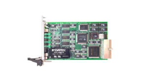
CPCI-6713-2IP
CPCI 320C6317B DSP Dual Industry Pack Carrier
The board features private SDRAM and Flash memory attached to the DSP, with an FPGA providing timing and control. It includes peripherals such as a serial port and connectors for IP mezzanine boards. The Flash memory allows for downloading programs into non-volatile memory. Additionally, a PCI bus connector serves as the interface to the host computer, facilitating communication and data transfer between the board and the host system.
Available Software Drivers and Software Tools:
- C library DLLs
- Linux drivers
- Windows XP drivers
- VxWorks drivers
- LabView
The TMS320C67x DSP generation is supported by the TI eXpressDSP™ set of industry development tools, including a highly optimizing C/C++ Compiler, the Code Composer Studio™ Integrated Development Environment (IDE), JTAG-based emulation, real-time debugging, and the DSP/BIOS™ kernel.
Applications:
For application requiring low cost, high density I/O or unique combinations, the CPCI-6713B-2IP is the perfect solution. The Local DSP can be used to simply move data to and from the CPCI bus or provide pre processing functions such as local PID controls, FFT’s, digital filtering, etc. Custom application software can be downloaded to the DSP via the CompactPCI bus.
TMS320C6713 DSP Features:
-
-
- TMS320C6713B™ DSP @ 300 MHz
- 32/64 bit data word
- 8 32-bit instructions/cycle
- Up to 2400 MIPS/MFLOPS
- Advanced very long instruction word DSP core with 8 independent functional units:
- 2 ALUs (fixed point)
- 4 ALUs (floating/fixed point)
- 2 multipliers (floating/fixed point)
- L1/L2 memory architecture:
- 4K byte L1P program cache
- 4K byte L1D data cache (2-way)
- 256K byte L2 memory total with 64KByte L2 Unified Cache/Mapped RAM
- 192K-Byte Additional L2 Mapped RAM
- Load-store architecture with 32 32-bit general-purpose registers
- Native instructions for IEEE 754 single and double precision operations
- 32-bit external memory interface with a glueless interface to SRAM, EPROM, Flash, SBSRAM, and SDRAM with 512 Mbyte total addressable external memory space
- Dual 32-bit general-purpose timers
- 16 channel EDMA ‘Enhanced DMA’
- Two inter-integrated circuit bus (I2C Bus)
- 16-bit Host-Port Interface (HPI)
- IEEE-1149.1 (JTAG) boundary scan compatible
-
Industry Pack Specifications:
-
-
- Dual Industry Pack Sites
- Meets ANSI Vita 4
- 8/32 MHz operation
- Support ID, I/O, Int. & mem spaces
- 2 Interrupts
- Hardware self-timed per IP module
- Triggered via system reset and software control
- Jumper or software time-out function
- 5, +/-12 volt reset-able fuse per IP
- 8/16 bit data
-
PCI Bus:
-
-
- PLX 9056 33/66MHz 32-bit, PCI r2.2 compliant
- Motorola PowerQUICC and generic 32-bit, 66MHz local bus modes
- 3.3V I/O, 5V tolerant bus interfaces
- PICMG 2.1 r2.0 hot swap
- Zero wait state burst operation, with PCI bus bursts to 264 MB/sec and local bus bursts to 264 MB/sec
- 2 DMA channels
- Direct master data transfers
- Direct slave data transfers
-
PCI Bus Control:
-
-
- I2O r1.5 messaging unit
- 8 mailboxes and 32 doorbell registers
- PCI arbiter supports 7 external masters
- Host mode reset/interrupt
- Power management event generation support
- Serial EEPROM interface
- JTAG boundary scan
-
Operating Environment:
-
-
- Operating temperature: Commercial: 0 to +70 ºC, Optional: -25 ºC to +80 ºC
- Non-operating temperature: -40 ºC to +85 ºC
- Airflow requirement – 5 CFM
- Humidity – 5 to 90% (non-condensing)
- Altitude – 0 to 10,000 feet
-
Mechanical & Environmental:
-
- Size – 3U CPCI module 100mm x 160mm
- Single wide PMC 2.92” X 5.87”
- Power – 1.5 watt
- Front panel I/O on carrier and mezzanine IP cards
- Vibration – 0.5G, 20-2000 Hz random
- Shock – 20G, 11 msec, ½ sine
- Weight – TBD
- MTBF – >250,000 hours
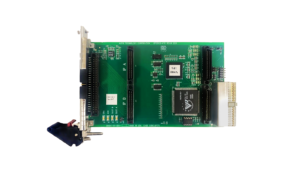
CPCI-6713B-2 IP:
3U industry pack carrier with 320C6713B DSP
Optional Accessories
CBL-50-HRS:
Cable
TB-50-HRS:
Terminal block
- Based around the Texas Instruments floating-point Digital Signal Processor TMS-320C6713
- Dual industry pack carrier configuration enabling a vast array of I/O possibilities, creating a cost-effective solution for DSP and I/O
- Compact PCI bus compatible
- Virtually unlimited customization of the input-output functions as well as hardware-accelerated signal processing
- Adds high-speed, low latency I/O and deterministic control to a low-cost PC system solution
| Mechanical Interface | Switched Mezzanine Card (XMC) Interface confirming to ANSI/VITA 42.0-2008 (Auxiliary Standard) Standard single-width (149mm x 74mm) | |||||||||
| Electrical Interface | PCI Express x4 Link (Base Specification 2.1) compliant interface conforming to ANSI/VITA 42.3-2006 (PCI Express Protocol Layer Standard) | |||||||||
| PCI Express Switch | PI7C9X2G312GP (Pericom) | |||||||||
| PCI Express to PCI Bridge | XIO2001 (Texas Instruments) | |||||||||
| User configurable FPGA | TXMC639-10R: XC7K160T-2FBG676I (AMD) TXMC639-11R: XC7K325T-2FBG676I (AMD) | |||||||||
| SPI-Flash | MT25QL128 (Micron) 128 Mbit (contains TXMC639 FPGA BRD) or compatible; +3.3 V supply voltage | |||||||||
| DDR3 RAM | 2x MT41K256M16TW-107 (Micron) 256Meg x 32 bit | |||||||||
| Board Configuration Controller | LCMXO2-7000HC (Lattice) | |||||||||
| ADC | LTC2320 -16 (Analog Devices) | |||||||||
| DAC | AD5547BRUZ (Analog Devices) | |||||||||
| A/D Channels | TXMC639-10R: 8 Differential 16bit A/D Channels TXMC639-11R: 16 Differential 16bit A/D Channels Input Configuration per BCC Device: Input Voltage Ranges: Differental : ±20.57 V, ±10.28 V or ±5.14 V (Single-Ended: ±10.28 V, ±5.14 V or ±2.57 V) All analog inputs are connected via an impedance converter and a second operation amplifier for level adjustment and filtering to the differential ADC inputs. The -3 dB limit of this input stage is at approx. 8MHz | |||||||||
| D/A Channels | TXMC639-10R: 4 Single-Ended 16 Bit D/A Channels TXMC639-11R: 8 Single-Ended 16 Bit D/A Channels Output range configurable per D/A channel. Maximum single-ended Output Voltage – Vout: ±10 V Maximum Output Drive Current for each Output: 10 mA Maximum Capacitive Load for each Output: 1000 pF Typical Settling Time for a 10 mA / 1000 pF: < 1 µs | |||||||||
| Digital Front I/O Channels | 32 digital I/O Lines
| |||||||||
| Digital Rear I/O Channels | 64 direct FPGA I/O lines to P14 Rear I/O connector
4 MGT line to P16 Rear I/O connector
| |||||||||
| Front I/O | Front I/O Samtec – ERF8_050_01_L_D_RA_L_TR | |||||||||
| P14 Rear I/O | 64 pin Mezzanine Connector (Molex 71436-2864 or compatible) | |||||||||
| P16 Rear I/O | 114 pin Mezzanine Connector (Samtec – ASP-105885-01) | |||||||||
| Power Requirements 1) | Depends on FPGA design With TXMC639 Board Reference Design / without external load
| |||||||||
| Temperature Range | Operating: – 40 °C to + 85 °C Storage: – 55 °C to + 125 °C | |||||||||
| MTBF 1) | 157 000 h to 161 000 h | |||||||||
| Humidity | 5% – 95% non-condensing | |||||||||
| Weight | 140 g |
1) depends on variant, for further details see User Manual
TXMC639-10R
| 8x Analog In, 4x Analog Out, XC7K160T-2FBG676 Kintex™ 7 FPGA AMD Kintex™ 7 FPGA (XC7K160T-2FBG676), 1GB DDR3, 8x Analog In, 4x Analog Out, 32x digital Front I/O, 64x direct FPGA Rear I/O Lines and 4x MGTs Rear I/O |
TXMC639-11R
| 16x Analog In, 8x Analog Out, XC7K325T-2FBG676 Kintex™ 7 FPGA AMD Kintex™ 7 FPGA (XC7K325T-2FBG676), 1GB DDR3, 16x Analog In, 8x Analog Out, 32x digital Front I/O, 64x direct FPGA Rear I/O Lines and 4x MGTs Rear I/O |
SOFTWARE
Share this product
LinkedIn