- Form Factor: XMC VITA 61 or VITA 42 options
- Interface: PCI Express x1 lane interface
- MIL-STD-1553 Controllers: Two dual redundant MIL-STD-1553 controllers (A/B channels)
- Multiprotocol Support: MIL-STD-1553A/B, STANAG-3838, and MIL-STD-1760
- Memory: 2MB RAM per channel
- Modes: Bus Controller, Remote Terminal with concurrent Bus Monitor
- Monitoring: IRIG-106 Chapter 10 Monitor
- RT Emulation: Emulates up to 31 RT addresses simultaneously
- Filtering: Filter based on RT address, T/R bit, sub-address
- Coupling: Transformer coupled
- IRIG-B Input: IRIG-B digital input
- Digital I/O: 16 digital discrete I/O (TTL Levels)
- Digital Outputs: 2 digital outputs


XMC-1553-2-IO
Two Channel Dual Redundant 1553 Controller, Multiple RT Support
- Form Factor: XMC VITA 61 or VITA 42 options
- Interface: PCI Express x1 lane interface
- MIL-STD-1553 Controllers: Two dual redundant MIL-STD-1553 controllers (A/B channels)
- Multiprotocol Support: MIL-STD-1553A/B, STANAG-3838, and MIL-STD-1760
- Memory: 2MB RAM per channel
- Modes: Bus Controller, Remote Terminal with concurrent Bus Monitor
- Monitoring: IRIG-106 Chapter 10 Monitor
- RT Emulation: Emulates up to 31 RT addresses simultaneously
- Filtering: Filter based on RT address, T/R bit, sub-address
- Coupling: Transformer coupled
- IRIG-B Input: IRIG-B digital input
- Digital I/O: 16 digital discrete I/O (TTL Levels)
- Digital Outputs: 2 digital outputs
Share this product
LinkedIn
XMC-1553-2-IO
Two Channel Dual Redundant 1553 Controller, Multiple RT Support
The XMC-1553-2-IO-2 uses a DDC Total-ACE communication device as its 1553 bus controller, or as a remote terminal with concurrent bus monitor terminal. Dual controller has a dual redundant channel with built-in transceivers and transformer. The controller has the capability to emulate up to 31 RT addresses simultaneously. The XMC-1553-2-IO Block Diagram shows that in RT mode, it can filter on RT address, T/R, sub-address. The board supports 16 digital I/O TTL Levels. The board format is full XMC VITA61 2011 or VITA42, and is provided in an extended temperature range.
Applications:
- Industrial and Military
- Test equipment supporting evaluation and simulation
- Operational equipment such as avionics, space satellite systems, aircraft onboard systems
- Commercial systems
- Monitoring and analysis
Available Software Drivers:
- C library dll’s
- Linux drivers
- Windows drivers
- VxWorks drivers
Ordering Information (Additional A/D Modules from image – Assumed no 1553 functionality):Commercial Temperature: 0°C to +70°C
- XMC-16AD16-200: 16 Channels 16 Bits, 200KSP
- XMC-32AD16-200: 32 Channels 16 Bits, 200KSP
Extended Temperature: -40°C to +85°C
- XMC-16AD16-200-I: 16 Channels 16 Bits, 200KSP
- XMC-32AD16-200-I: 32 Channels 16 Bits, 200KSP
Optional Accessories:
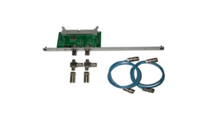
- CBL-XMC-1553-2-12: 12 inch 1553 cable to 4 Triax
- Form Factor: XMC VITA 61 or VITA 42 options
- Interface: PCI Express x1 lane interface
- MIL-STD-1553 Controllers: Two dual redundant MIL-STD-1553 controllers (A/B channels)
- Multiprotocol Support: MIL-STD-1553A/B, STANAG-3838, and MIL-STD-1760
- Memory: 2MB RAM per channel
- Modes: Bus Controller, Remote Terminal with concurrent Bus Monitor
- Monitoring: IRIG-106 Chapter 10 Monitor
- RT Emulation: Emulates up to 31 RT addresses simultaneously
- Filtering: Filter based on RT address, T/R bit, sub-address
- Coupling: Transformer coupled
- IRIG-B Input: IRIG-B digital input
- Digital I/O: 16 digital discrete I/O (TTL Levels)
- Digital Outputs: 2 digital outputs
| Mechanical Interface | Switched Mezzanine Card (XMC) Interface confirming to ANSI/VITA 42.0-2008 (Auxiliary Standard) Standard single-width (149mm x 74mm) | |||||||||
| Electrical Interface | PCI Express x4 Link (Base Specification 2.1) compliant interface conforming to ANSI/VITA 42.3-2006 (PCI Express Protocol Layer Standard) | |||||||||
| PCI Express Switch | PI7C9X2G312GP (Pericom) | |||||||||
| PCI Express to PCI Bridge | XIO2001 (Texas Instruments) | |||||||||
| User configurable FPGA | TXMC639-10R: XC7K160T-2FBG676I (AMD) TXMC639-11R: XC7K325T-2FBG676I (AMD) | |||||||||
| SPI-Flash | MT25QL128 (Micron) 128 Mbit (contains TXMC639 FPGA BRD) or compatible; +3.3 V supply voltage | |||||||||
| DDR3 RAM | 2x MT41K256M16TW-107 (Micron) 256Meg x 32 bit | |||||||||
| Board Configuration Controller | LCMXO2-7000HC (Lattice) | |||||||||
| ADC | LTC2320 -16 (Analog Devices) | |||||||||
| DAC | AD5547BRUZ (Analog Devices) | |||||||||
| A/D Channels | TXMC639-10R: 8 Differential 16bit A/D Channels TXMC639-11R: 16 Differential 16bit A/D Channels Input Configuration per BCC Device: Input Voltage Ranges: Differental : ±20.57 V, ±10.28 V or ±5.14 V (Single-Ended: ±10.28 V, ±5.14 V or ±2.57 V) All analog inputs are connected via an impedance converter and a second operation amplifier for level adjustment and filtering to the differential ADC inputs. The -3 dB limit of this input stage is at approx. 8MHz | |||||||||
| D/A Channels | TXMC639-10R: 4 Single-Ended 16 Bit D/A Channels TXMC639-11R: 8 Single-Ended 16 Bit D/A Channels Output range configurable per D/A channel. Maximum single-ended Output Voltage – Vout: ±10 V Maximum Output Drive Current for each Output: 10 mA Maximum Capacitive Load for each Output: 1000 pF Typical Settling Time for a 10 mA / 1000 pF: < 1 µs | |||||||||
| Digital Front I/O Channels | 32 digital I/O Lines
| |||||||||
| Digital Rear I/O Channels | 64 direct FPGA I/O lines to P14 Rear I/O connector
4 MGT line to P16 Rear I/O connector
| |||||||||
| Front I/O | Front I/O Samtec – ERF8_050_01_L_D_RA_L_TR | |||||||||
| P14 Rear I/O | 64 pin Mezzanine Connector (Molex 71436-2864 or compatible) | |||||||||
| P16 Rear I/O | 114 pin Mezzanine Connector (Samtec – ASP-105885-01) | |||||||||
| Power Requirements 1) | Depends on FPGA design With TXMC639 Board Reference Design / without external load
| |||||||||
| Temperature Range | Operating: – 40 °C to + 85 °C Storage: – 55 °C to + 125 °C | |||||||||
| MTBF 1) | 157 000 h to 161 000 h | |||||||||
| Humidity | 5% – 95% non-condensing | |||||||||
| Weight | 140 g |
1) depends on variant, for further details see User Manual
TXMC639-10R
| 8x Analog In, 4x Analog Out, XC7K160T-2FBG676 Kintex™ 7 FPGA AMD Kintex™ 7 FPGA (XC7K160T-2FBG676), 1GB DDR3, 8x Analog In, 4x Analog Out, 32x digital Front I/O, 64x direct FPGA Rear I/O Lines and 4x MGTs Rear I/O |
TXMC639-11R
| 16x Analog In, 8x Analog Out, XC7K325T-2FBG676 Kintex™ 7 FPGA AMD Kintex™ 7 FPGA (XC7K325T-2FBG676), 1GB DDR3, 16x Analog In, 8x Analog Out, 32x digital Front I/O, 64x direct FPGA Rear I/O Lines and 4x MGTs Rear I/O |
SOFTWARE
Share this product
LinkedIn