- 1 or 2 controller of dual redundant (A/B channel) 1553 communications
- Programmable bus controller, remote terminal, or monitor terminal modes
- MIL-STD-1553 A and B compliant, Notice 2 RT
- Long or short stub support
- Low power consumption
- PCIMG compliant
- +3.3V or +5 VDC VIO
- LED status
- Selectable external or internal clock


PCI-1553-X-PLX-SB
Single/Dual UTMC SµMMIT DXE 1553 Controller
- 1 or 2 controller of dual redundant (A/B channel) 1553 communications
- Programmable bus controller, remote terminal, or monitor terminal modes
- MIL-STD-1553 A and B compliant, Notice 2 RT
- Long or short stub support
- Low power consumption
- PCIMG compliant
- +3.3V or +5 VDC VIO
- LED status
- Selectable external or internal clock
Share this product
LinkedIn
PCI-1553-X-PLX-SB
Single/Dual UTMC SµMMIT DXE 1553 Controller
The PCI-1553-x-PLX-SB uses a single UTMC’s Sµmmit DXE UT69151DXE-GPC 1553 communication device as its 1553 bus controller, or remote terminal, or monitor terminal. The single controller has two redundant channels. This controller accesses 64Kx16 word of external memory and has internal transceivers for both channel A and B. The PCI board has on-board transformers for both channels.
Available Software Drivers:
-
-
- C library dll’s
- Linux drivers
- Windows XP drivers
- VxWorks drivers
-
Applications:
This is a perfect solution for a wide array of 1553 communication applications such as:
-
-
- Test equipment supporting evaluation, simulation, monitoring, and analysis
- Operational equipment such as avionics, space satellite systems, aircraft onboard systems, commercial systems, etc.
- Applications that require dual functionality of the terminal for monitoring and remote operation at the same time
-
1553 Compliance/Characteristics:
-
-
- Data Rate – 1 MHz
- Word Length – 20 bits
- Data Bits/Word – 16 bits
- Message Length – maximum of 32 data words
- Transmission Technique – half-duplex
- Operation – asynchronous
- Transmission encoding – Manchester II, biphase
- Protocol – command/response
- Bus Control – single or multiple
- Fault tolerance – typically dual redundant, second bus in “hot backup” status
- Message formats – controller to terminal, terminal to controller, terminal to terminal, broadcast, system control
- Number of remote terminals – maximum 31
- Terminal Types – remote terminal, bus controller, bus monitor
- Transmission Media – twisted shielded pair
- Coupling – transformer and direct
-
UTMC/Summit /DXE Features:
-
-
- Integrated transceivers
- RT mode internal command illegalization
- 16-bit read/write time-tag with user-defined resolution
- Sub-address data buffering
- Simultaneous RT/MT mode of operation
- BC architecture designed with:
- Minor frame timing
- Efficient command block flow statements
- Status word polling
- Programmable retries
- Programmable interrupt architecture
- Autonomous operation in all three modes
-
PCI Bus:
-
-
- PCI Bus Interface 3.3VDC/5VDC
- PLX 9080 33/66MHz 32-bit, PCI r2.2 compliant
- 3.3V I/O, 5V tolerant bus interfaces
- PICMG 2.1 r2.0 hot swap
- Zero wait state burst operation, with PCI bus bursts to 264 MB/sec and local bus bursts to 264 MB/sec
- 2 DMA channels
- Direct master data transfers
- Direct slave data transfers
- 33 MHz clock
- 16-bit address
- 16-bit data
- FIFO support burst operations
-
PCI Bus Control:
-
-
- I2O r1.5 messaging unit
- 8 mailboxes and 32 doorbell registers
- PCI arbiter supports 7 external masters
- Host mode reset/interrupt
- Big endian/little endian conversions
- Power management event generation support
- Serial EEPROM interface
- JTAG boundary scan, RS-232 RJ45
-
Operating Environment:
-
-
- Operating temperature:
- Commercial: 0 to +70 ºC
- Industrial: -40 ºC to +85 ºC
- Non-operating: -45 ºC to +95 ºC
- Airflow requirement – 5 CFM
- Humidity – 5 to 90% (non-cond.)
- Altitude – 0 to 10,000 feet
- Operating temperature:
-
Mechanical: Environmental:
-
-
- Size – ½ PCI card
- Power – 1.5 watt
- Front panel or rear panel I/O
- Vibration – 0.5G, 20-2000 Hz rand
- Shock – 20G, 11 msec, ½ sine
- Weight – TBD
- MTBF – >250,000 hours\
-
Terminal Electrical Input Characteristics:
Requirements:
-
-
- Transformer coupled: 0.866-14.0V
- Direct Coupled: 1.2-20.0V
- No response:
- Transformer coupled: 0.0-0.2V
- Direct Coupled: 0.0-0.28V
- Zero crossing stability: ±150.0 nSec
- Rise/fall times: 0 nsec – Sine
- Noise rejection: 140 mV WGN
- Common mode rejection: ±10.0V peak
- Input impedance: 1000 ohms (Transformer), 2000 ohms (Direct)
-
Terminal Electrical Output Characteristics:
Requirements:
-
- Transformer coupled: 18.0-27.0V
- Direct Coupled: 6.0-9.0V
- Zero crossing stability: 25.0 nsec
- Rise/fall: 100-300 nsec
- Max distortion: ±900.0 mV (Transformer), ±300.0 mV (Direct)
- Max output noise: 14.0 mV (Transformer), 5.0 mV (Direct)
- Max residual voltage: ±250.0 mV (Transformer), ±90.0 mV (Direct)
Optional Accessories
- Part Number: PCI-1553-1-PLX-SB
MIL-1553, 1 Channel Dual Redundant Summit - Part Number: PCI-1553-2-PLX-SB
MIL-1553, 2 Channels Dual Redundant Summit - Part Number: PCI-1553-X-PLX-SBI
Same as above with -40 to +85°C temperature rating
Optional Accessories
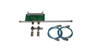
- Part Number: EngKit-1553 2
T’s, 2 Terminators, 2-1 meter cables - Part Number: CBL-1553-1
Standard-standard 2 meter 1553 cable - Part Number: CBL-1553-2
Standard-mini 2 meter 1553 cable
- 1 or 2 controller of dual redundant (A/B channel) 1553 communications
- Programmable bus controller, remote terminal, or monitor terminal modes
- MIL-STD-1553 A and B compliant, Notice 2 RT
- Long or short stub support
- Low power consumption
- PCIMG compliant
- +3.3V or +5 VDC VIO
- LED status
- Selectable external or internal clock
| Mechanical Interface | Switched Mezzanine Card (XMC) Interface confirming to ANSI/VITA 42.0-2008 (Auxiliary Standard) Standard single-width (149mm x 74mm) | |||||||||
| Electrical Interface | PCI Express x4 Link (Base Specification 2.1) compliant interface conforming to ANSI/VITA 42.3-2006 (PCI Express Protocol Layer Standard) | |||||||||
| PCI Express Switch | PI7C9X2G312GP (Pericom) | |||||||||
| PCI Express to PCI Bridge | XIO2001 (Texas Instruments) | |||||||||
| User configurable FPGA | TXMC639-10R: XC7K160T-2FBG676I (AMD) TXMC639-11R: XC7K325T-2FBG676I (AMD) | |||||||||
| SPI-Flash | MT25QL128 (Micron) 128 Mbit (contains TXMC639 FPGA BRD) or compatible; +3.3 V supply voltage | |||||||||
| DDR3 RAM | 2x MT41K256M16TW-107 (Micron) 256Meg x 32 bit | |||||||||
| Board Configuration Controller | LCMXO2-7000HC (Lattice) | |||||||||
| ADC | LTC2320 -16 (Analog Devices) | |||||||||
| DAC | AD5547BRUZ (Analog Devices) | |||||||||
| A/D Channels | TXMC639-10R: 8 Differential 16bit A/D Channels TXMC639-11R: 16 Differential 16bit A/D Channels Input Configuration per BCC Device: Input Voltage Ranges: Differental : ±20.57 V, ±10.28 V or ±5.14 V (Single-Ended: ±10.28 V, ±5.14 V or ±2.57 V) All analog inputs are connected via an impedance converter and a second operation amplifier for level adjustment and filtering to the differential ADC inputs. The -3 dB limit of this input stage is at approx. 8MHz | |||||||||
| D/A Channels | TXMC639-10R: 4 Single-Ended 16 Bit D/A Channels TXMC639-11R: 8 Single-Ended 16 Bit D/A Channels Output range configurable per D/A channel. Maximum single-ended Output Voltage – Vout: ±10 V Maximum Output Drive Current for each Output: 10 mA Maximum Capacitive Load for each Output: 1000 pF Typical Settling Time for a 10 mA / 1000 pF: < 1 µs | |||||||||
| Digital Front I/O Channels | 32 digital I/O Lines
| |||||||||
| Digital Rear I/O Channels | 64 direct FPGA I/O lines to P14 Rear I/O connector
4 MGT line to P16 Rear I/O connector
| |||||||||
| Front I/O | Front I/O Samtec – ERF8_050_01_L_D_RA_L_TR | |||||||||
| P14 Rear I/O | 64 pin Mezzanine Connector (Molex 71436-2864 or compatible) | |||||||||
| P16 Rear I/O | 114 pin Mezzanine Connector (Samtec – ASP-105885-01) | |||||||||
| Power Requirements 1) | Depends on FPGA design With TXMC639 Board Reference Design / without external load
| |||||||||
| Temperature Range | Operating: – 40 °C to + 85 °C Storage: – 55 °C to + 125 °C | |||||||||
| MTBF 1) | 157 000 h to 161 000 h | |||||||||
| Humidity | 5% – 95% non-condensing | |||||||||
| Weight | 140 g |
1) depends on variant, for further details see User Manual
TXMC639-10R
| 8x Analog In, 4x Analog Out, XC7K160T-2FBG676 Kintex™ 7 FPGA AMD Kintex™ 7 FPGA (XC7K160T-2FBG676), 1GB DDR3, 8x Analog In, 4x Analog Out, 32x digital Front I/O, 64x direct FPGA Rear I/O Lines and 4x MGTs Rear I/O |
TXMC639-11R
| 16x Analog In, 8x Analog Out, XC7K325T-2FBG676 Kintex™ 7 FPGA AMD Kintex™ 7 FPGA (XC7K325T-2FBG676), 1GB DDR3, 16x Analog In, 8x Analog Out, 32x digital Front I/O, 64x direct FPGA Rear I/O Lines and 4x MGTs Rear I/O |
SOFTWARE
Share this product
LinkedIn