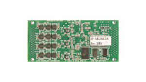
IP-DIO32P

IP Programmable Digital I/O, 32 channels

I/O Specifications:

  • Up to 32 I/O pins available in groups of 8 I/O pins.
  • All I/O can be individually programmed as an input or output via an Altera FPGA.
  • Direct read-back outputs on any or all outputs.

VMOSFET Specifications:

  • Open drain VMOSFET can sink up to 1.5A continuously.
  • Breakdown voltage of 50V.
  • Wide input voltage range up to +30VDC.
  • Very low Ron (0.3Ω) for reduced heat dissipation.

Share this product

LinkedIn

Got Questions?

IP-DIO32P

IP Programmable Digital I/O, 32 channels

I/O Specifications:

  • Up to 32 I/O pins available in groups of 8 I/O pins.
  • All I/O can be individually programmed as an input or output via an Altera FPGA.
  • Direct read-back outputs on any or all outputs.

VMOSFET Specifications:

  • Open drain VMOSFET can sink up to 1.5A continuously.
  • Breakdown voltage of 50V.
  • Wide input voltage range up to +30VDC.
  • Very low Ron (0.3Ω) for reduced heat dissipation.

The IP-DIO32P module features 32 Altera-based programmable I/O pins, capable of handling voltages up to +30VDC. These pins are organized into groups of 8, allowing for flexible configuration and control. Each output pin supports read-back functionality, enabling the system to monitor its current state. The inputs have variable thresholds and can handle contact and switched voltages, with a resistor network-based variable hysteresis to enhance noise immunity. The input voltage reference can be selected from +5VDC, ground, or an external reference, providing versatility in handling different input voltage levels. A 2Kbyte EEPROM is included for storing the board ID, user data, and potential gain error corrections for future software updates.

Industry Pack Specifications
  • Meets ANSI/VITA 4-1995
  • 8/32 MHz synchronous operation
  • Supports ID, 128 byte I/O, interrupt, & 8 Mbyte memory spaces
  • 2 Interrupts per module
  • Two passive DMA channels are possible
  • Hardware self timed per IP module
  • Triggered via system reset and software control
  • Jumper or software time-out function
  • 5, +/-12 volt reset-able fuse per IP
Mechanical: Environmental
  • Size – VITA 4 compliant: 1.8″ x 3.9″ or 46 mm x 99 mm
  • Power – 1.0 watt
  • Vibration – 0.5G, 20-2000 Hz rand
  • Shock – 20G, 11 msec, 1⁄2 sine
  • Weight – tbd
  • MTBF – >250,000 hours
Operating Environment
  • Operating temperature
    • Commercial: 0 to +70°C
    • Optional: -25°C to +80°C
  • Non-operating: -40°C to +85°C
  • Airflow requirement – 5 CFM
  • Humidity – 5 to 90% (non-condensing)
  • Altitude – 0 to 10,000 feet

Ordering Information:

  • IP-DIO32P-I: 32-bit digital I/O Industry Pack module, operating at -40º to +85ºC

Optional Accessories:

  • CBL-HDR-HRS-50: 50 pin cable, 1 meter with HRS connector
  • TB-HDR-50: 50 pin terminal block

Data Sheet – Link Here

User Manual – Link Here

I/O Specifications:
  • Up to 32 I/O pins available in groups of 8 I/O pins.
  • All I/O can be individually programmed as an input or output via an Altera FPGA.
  • Direct read-back outputs on any or all outputs.
VMOSFET Specifications:
  • Open drain VMOSFET can sink up to 1.5A continuously.
  • Breakdown voltage of 50V.
  • Wide input voltage range up to +30VDC.
  • Very low Ron (0.3Ω) for reduced heat dissipation.


Mechanical Interface

Switched Mezzanine Card (XMC) Interface confirming to ANSI/VITA 42.0-2008 (Auxiliary Standard)

Standard single-width (149mm x 74mm)

Electrical InterfacePCI Express x4 Link (Base Specification 2.1) compliant interface conforming to ANSI/VITA 42.3-2006 (PCI Express Protocol Layer Standard)
PCI Express SwitchPI7C9X2G312GP (Pericom)
PCI Express to PCI BridgeXIO2001 (Texas Instruments)
User configurable FPGA

TXMC639-10R: XC7K160T-2FBG676I (AMD)

TXMC639-11R: XC7K325T-2FBG676I (AMD)

SPI-FlashMT25QL128 (Micron) 128 Mbit (contains TXMC639 FPGA BRD) or compatible; +3.3 V supply voltage
DDR3 RAM2x MT41K256M16TW-107 (Micron) 256Meg x 32 bit
Board Configuration ControllerLCMXO2-7000HC (Lattice)
ADCLTC2320 -16 (Analog Devices)
DACAD5547BRUZ (Analog Devices)
A/D Channels

TXMC639-10R: 8 Differential 16bit A/D Channels

TXMC639-11R: 16 Differential 16bit A/D Channels

Input Configuration per BCC Device:

Input Voltage Ranges:

Differental : ±20.57 V, ±10.28 V or ±5.14 V

(Single-Ended: ±10.28 V, ±5.14 V or ±2.57 V)

All analog inputs are connected via an impedance converter and a second operation amplifier for level adjustment and filtering to the differential ADC inputs.

The -3 dB limit of this input stage is at approx. 8MHz

D/A Channels

TXMC639-10R: 4 Single-Ended 16 Bit D/A Channels

TXMC639-11R: 8 Single-Ended 16 Bit D/A Channels

Output range configurable per D/A channel.
Simultaneous Conversion for all D/A Channels.

Maximum single-ended Output Voltage – Vout: ±10 V

Maximum Output Drive Current for each Output: 10 mA

Maximum Capacitive Load for each Output: 1000 pF

Typical Settling Time for a 10 mA / 1000 pF: < 1 µs

Digital Front I/O Channels

32 digital I/O Lines

  • Default configured as 32 ESD-protected TTL lines
  • 16 I/O lines are configurable as 8 differential RS422 I/O lines with individual Termination enable.
Digital Rear I/O Channels

64 direct FPGA I/O lines to P14 Rear I/O connector

  • Can be used as single-ended or differential I/O
  • FPGA I/O Standard: LVCMOS25, LVTTL25 and LVDS25

4 MGT line to P16 Rear I/O connector

  • Each line consists of one differential RX and TX pair.
  • Transmission speeds of up to 3.125 Gb/s are possible.
Front I/OFront I/O Samtec – ERF8_050_01_L_D_RA_L_TR
P14 Rear I/O64 pin Mezzanine Connector (Molex 71436-2864 or compatible)
P16 Rear I/O114 pin Mezzanine Connector (Samtec – ASP-105885-01)
Power Requirements 1)

Depends on FPGA design

With TXMC639 Board Reference Design / without external load

 typical @ +12 V VPWRtypical @ +5 V VPWR
TXMC639-10R1.1 A2.5 A
TXMC639-11R1.3 A3.3 A
Temperature RangeOperating: – 40 °C to + 85 °C
Storage: – 55 °C to + 125 °C
MTBF 1)157 000 h to 161 000 h
Humidity5% – 95% non-condensing
Weight140 g

1) depends on variant, for further details see User Manual


TXMC639-10R


8x Analog In, 4x Analog Out, XC7K160T-2FBG676 Kintex™ 7 FPGA

AMD Kintex™ 7 FPGA (XC7K160T-2FBG676), 1GB DDR3, 8x Analog In, 4x Analog Out, 32x digital Front I/O, 64x direct FPGA Rear I/O Lines and 4x MGTs Rear I/O

TXMC639-11R


16x Analog In, 8x Analog Out, XC7K325T-2FBG676 Kintex™ 7 FPGA

AMD Kintex™ 7 FPGA (XC7K325T-2FBG676), 1GB DDR3, 16x Analog In, 8x Analog Out, 32x digital Front I/O, 64x direct FPGA Rear I/O Lines and 4x MGTs Rear I/O

SOFTWARE

Device Driver for Board Family with Reconfigurable FPGA

Data Sheet – Link-Here

User Manual – Link-Here

Share this product

LinkedIn
Scroll to Top

User Manual Request

Please submit your information & we will send you a link and password to access our product manual. 

Please submit your information & we will send you a link and password to access our product manual. 

Already have a password? Visit manuals page below.

Already have a password?
Visit manuals page below.