- Altera Cyclone IV FPGA EP4CE30, 55, 75, 115
- Stand alone possibility
- Single wide Industry Pack
- 20 Mbps RS485
- Logic-Selectable 120Ω Termination Resistor
- Optional User clock oscillator


IP-CYCLONE-IV-PIO
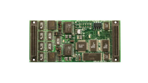
USER RECONFIGURABLE ALTERA CYCLONE IV 64MBYTES DUAL-PORTED DDR RS-422/485, TTL OR COMBINATION I/O DRIVERS
- Altera Cyclone IV FPGA EP4CE30, 55, 75, 115
- Stand alone possibility
- Single wide Industry Pack
- 20 Mbps RS485
- Logic-Selectable 120Ω Termination Resistor
- Optional User clock oscillator
Share this product
LinkedIn
IP-CYCLONE-IV-PIO
USER RECONFIGURABLE ALTERA CYCLONE IV 64MBYTES DUAL-PORTED DDR RS-422/485, TTL OR COMBINATION I/O DRIVERS
This advanced FPGA module is powered by the Altera Cyclone IV with 484-pin options available in CE30, 55, 75, and 115 configurations. Designed as a compatible upgrade to the Alphi IP-CycloneII, it offers increased flexibility and performance for demanding embedded system applications. The board features 32 Mbytes of DDR memory and dual-ported SRAM for high-speed data access and efficient multitasking. A dedicated logic block manages the IP interface, ensuring seamless communication between system components. With 48 reconfigurable I/O lines organized into 24 differential pairs, the module supports a wide range of connectivity options. These lines are equipped with RS-422/485 drivers and can be grouped in sets of 4 (2 pairs) for user-configurable setups. Additionally, the board features software-programmable 120-ohm termination, allowing for flexible signal conditioning.
Programming the device is straightforward, with support for both IP bus programming and bit/byte blaster methods. The inclusion of a local serial EPROM allows for efficient booting and storage of configuration data.
For precise timing requirements, the module supports both internal and external clocking, with 8 MHz and 32 MHz IP clock support. Fully VITA 4 compliant, this FPGA module offers a versatile, high-performance solution for a range of industrial, aerospace, and defense applications.
Memory:
-
- 64 Mbyte external DDR
- Dual ported between the Altera and IP bus with arbitration
I/O Level:
-
- 24 pair RS-422/485 or 48 TTL or a combination
- 20 Mbps RS485
- High Input Impedance Supports 256 Nodes
- Software-Selectable, Half/Full-Duplex
- Enhanced ESD protection allows to withstand ±15kV
- Logic-Selectable 120Ω Termination Resistor
Cyclone IV Programmable via:
-
- Bit / Byte Blaster
- Serial EPROM
- IP Bus
IP Interface:
-
- 8/32 MHz clock
- 16-bit address
- Interrupts
Operating: Environmental:
-
- Operating temperature:
- Commercial: 0 to +55 °C
- Optional: -40°C to +85°C
- Airflow requirement: 0.5 CFM
- Humidity: 5 to 90% (non-cond.)
- Altitude: 0 to 10,000 ft
- Operating temperature:
Mechanical: Environmental:
-
- Size: Vita 4 Type 1 IP – 1.8” x 3.9”
- Power: 1 watt
- Vibration: 0.5G RMS, 20-2000 Hz random
- Shock: 20 G, 11 ms, ½ sine
- Weight: TBD
- MTBF: >250,000 hours
Ordering Information:
- Part Number:
- IP-CIV-CE30-x – RS-485/422 ALTERA EP4CE30 Industry Pack module
- IP-CIV-CE55-x – RS-485/422 ALTERA EP4CE55 Industry Pack module
- IP-CIV-CE75-x – RS-485/422 ALTERA EP4CE75 Industry Pack module
- IP-CIV-CE115-x – RS-485/422 ALTERA EP4CE115 Industry Pack module
- C Commercial : 0°C to 70°C
- I Industrial : -40°C to 85°C
Optional Accessories:
- Part Number:
- TB-50-HDR – 50 pin terminal block and 1 meter flat ribbon cable
- CBL-50-HDR – 50 pin, 1 meter flat ribbon cable, IDC header connector
- Altera Cyclone IV FPGA EP4CE30, 55, 75, 115
- Stand alone possibility
- Single wide Industry Pack
- 20 Mbps RS485
- Logic-Selectable 120Ω Termination Resistor
- Optional User clock oscillator
| Mechanical Interface | Switched Mezzanine Card (XMC) Interface confirming to ANSI/VITA 42.0-2008 (Auxiliary Standard) Standard single-width (149mm x 74mm) | |||||||||
| Electrical Interface | PCI Express x4 Link (Base Specification 2.1) compliant interface conforming to ANSI/VITA 42.3-2006 (PCI Express Protocol Layer Standard) | |||||||||
| PCI Express Switch | PI7C9X2G312GP (Pericom) | |||||||||
| PCI Express to PCI Bridge | XIO2001 (Texas Instruments) | |||||||||
| User configurable FPGA | TXMC639-10R: XC7K160T-2FBG676I (AMD) TXMC639-11R: XC7K325T-2FBG676I (AMD) | |||||||||
| SPI-Flash | MT25QL128 (Micron) 128 Mbit (contains TXMC639 FPGA BRD) or compatible; +3.3 V supply voltage | |||||||||
| DDR3 RAM | 2x MT41K256M16TW-107 (Micron) 256Meg x 32 bit | |||||||||
| Board Configuration Controller | LCMXO2-7000HC (Lattice) | |||||||||
| ADC | LTC2320 -16 (Analog Devices) | |||||||||
| DAC | AD5547BRUZ (Analog Devices) | |||||||||
| A/D Channels | TXMC639-10R: 8 Differential 16bit A/D Channels TXMC639-11R: 16 Differential 16bit A/D Channels Input Configuration per BCC Device: Input Voltage Ranges: Differental : ±20.57 V, ±10.28 V or ±5.14 V (Single-Ended: ±10.28 V, ±5.14 V or ±2.57 V) All analog inputs are connected via an impedance converter and a second operation amplifier for level adjustment and filtering to the differential ADC inputs. The -3 dB limit of this input stage is at approx. 8MHz | |||||||||
| D/A Channels | TXMC639-10R: 4 Single-Ended 16 Bit D/A Channels TXMC639-11R: 8 Single-Ended 16 Bit D/A Channels Output range configurable per D/A channel. Maximum single-ended Output Voltage – Vout: ±10 V Maximum Output Drive Current for each Output: 10 mA Maximum Capacitive Load for each Output: 1000 pF Typical Settling Time for a 10 mA / 1000 pF: < 1 µs | |||||||||
| Digital Front I/O Channels | 32 digital I/O Lines
| |||||||||
| Digital Rear I/O Channels | 64 direct FPGA I/O lines to P14 Rear I/O connector
4 MGT line to P16 Rear I/O connector
| |||||||||
| Front I/O | Front I/O Samtec – ERF8_050_01_L_D_RA_L_TR | |||||||||
| P14 Rear I/O | 64 pin Mezzanine Connector (Molex 71436-2864 or compatible) | |||||||||
| P16 Rear I/O | 114 pin Mezzanine Connector (Samtec – ASP-105885-01) | |||||||||
| Power Requirements 1) | Depends on FPGA design With TXMC639 Board Reference Design / without external load
| |||||||||
| Temperature Range | Operating: – 40 °C to + 85 °C Storage: – 55 °C to + 125 °C | |||||||||
| MTBF 1) | 157 000 h to 161 000 h | |||||||||
| Humidity | 5% – 95% non-condensing | |||||||||
| Weight | 140 g |
1) depends on variant, for further details see User Manual
TXMC639-10R
| 8x Analog In, 4x Analog Out, XC7K160T-2FBG676 Kintex™ 7 FPGA AMD Kintex™ 7 FPGA (XC7K160T-2FBG676), 1GB DDR3, 8x Analog In, 4x Analog Out, 32x digital Front I/O, 64x direct FPGA Rear I/O Lines and 4x MGTs Rear I/O |
TXMC639-11R
| 16x Analog In, 8x Analog Out, XC7K325T-2FBG676 Kintex™ 7 FPGA AMD Kintex™ 7 FPGA (XC7K325T-2FBG676), 1GB DDR3, 16x Analog In, 8x Analog Out, 32x digital Front I/O, 64x direct FPGA Rear I/O Lines and 4x MGTs Rear I/O |
SOFTWARE
Share this product
LinkedIn