- The IP-CIP-32 uses two Zilog Z8536 counter/timer and parallel I/O devices.
- 16 bits of bidirectional, double buffered I/O from each CIO for a total of 32 bits can be bit programmable as input or output.
- Six, 16-bit counter/timers total are available.
- Timer port #1 and #2 take over 2 lines of the 8-bit port B.
- Two special 4-bit ports for handshake support for port A and B and timer port #3 output.
- All three timers can be linked together.
- Multiple interrupt sources including pattern matching on ports A and B.
- Total of 8 interrupt lines available.
- 8 or 32 MHz clock.
- 2 interrupts and 2 slave DMA IP bus lines.
- VITA 4 compliant.
- 2kbytes of EEPROM are used for board ID and user data storage.


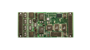
IP-CIO-32
P Counter/Timer & Parallel I/O
- The IP-CIP-32 uses two Zilog Z8536 counter/timer and parallel I/O devices.
- 16 bits of bidirectional, double buffered I/O from each CIO for a total of 32 bits can be bit programmable as input or output.
- Six, 16-bit counter/timers total are available.
- Timer port #1 and #2 take over 2 lines of the 8-bit port B.
- Two special 4-bit ports for handshake support for port A and B and timer port #3 output.
- All three timers can be linked together.
- Multiple interrupt sources including pattern matching on ports A and B.
- Total of 8 interrupt lines available.
- 8 or 32 MHz clock.
- 2 interrupts and 2 slave DMA IP bus lines.
- VITA 4 compliant.
- 2kbytes of EEPROM are used for board ID and user data storage.
Share this product
LinkedIn
IP-CIO-32
P Counter/Timer & Parallel I/O
Block Diagram and Operational Overview The IP-CIO-32 IP board has two Z8536 CIO’s from Zilog. The CIO consists of a CPU interface, three I/0 ports – A, B, and C – that consist of two general purpose 8-bit ports and one special purpose 4-bit port, three 16-bit counter/timers, an interrupt control logic block, and an internal control logic block. Both ports A and B include pattern recognition logic which allows interrupt generation when a specific pattern is detected. The pattern recognition logic can be programmed to make the port function like a priority interrupt controller. These same two ports can be concantenated to form a 16-bit word with handshake. The function of the special-purpose 4-bit port C depends upon the roles of ports A and B. Port C provides handshake lines when required by the other two ports. Port C also supports synchronization with DMA’s or CPUs. Port C has up to four port pins that can be used as dedicated external access lines for each counter/timer. Three different counter/timer output duty cycles are available – pulse, one-shot, and square-wave. The counter/timers can be programmed as either retriggerable or non-retriggerable. A 2kbyte EEPROM is used for the board ID and user data.
Applications
- This is a perfect solution for:
- Control systems
Z8536 CIO Device Specifications
- Two independent 8-bit, double-buffered, bidirectional I/O ports A and B
- Special 4-bit purpose I/O port C
- Programmable polarity, programmable direction in bit mode, “pulse catchers,” and programmable open-drain outputs for ports A and B
- Four handshake modes for port C supporting ports A and B, including 3-wire ala IEEE488 or REQUEST/WAIT signal for high-speed data transfer (DMA, CPU, etc.)
- Flexible pattern recognition logic, programmable as a 16-vector interrupt controller
- Three independent 16-bit counter/timers with up to four external access lines per counter/timer – count input, output, gate, and trigger
- Three output duty cycles for the counter/timer – pulsed, one-shot, and square-wave
- All internal registers (command, status, and data) are readable and writable except for the status bits
- All data registers can be directly accessed in a single operation
- VIH input high voltage = 2.0VDC min
- VIL output low voltage = 0.8VDC max
- VOH output high voltage = 2.4VDC min
- VOL output low voltage = 0.4VDC with IOL = 2.0mA
Industry Pack Specifications
- Meets ANSI/VITA 4-1995
- 8/32 MHz synchronous operation
- Supports ID, 128 byte I/O, interrupt, & 8 Mbyte memory spaces
- 2 Interrupts per module
- Two passive DMA channels are possible.
- Hardware self-timed per IP module
- Triggered via system reset and software control
- Jumper or software time-out function
- 5, +/-12 volt reset-able fuse per IP
Mechanical: Environmental
- Size – VITA 4 compliant: 1.8” x 3.9” or 46 mm x 99 mm
- Power – 1.0 watt
- Vibration – 0.5G, 20-2000 Hz rand
- Shock – 20G, 11 msec, 1⁄2 sine
- Weight – tbd
- MTBF – >250,000 hours
Operating Environment
- Operating temperature
Commercial: 0 to +70 °C
Optional: -25 °C to +80 °C - Non-operating: -40 °C to +85 °C
- Airflow requirement – 5 CFM
- Humidity – 5 to 90% (non-condensing)
- Altitude – 0 to 10,000 feet
Part Numbers:
- IP-CIO-32
- TB-50-HDR
Ordering Information:
- IP-CIO-32-1: Dual Z8536 CIO-based Industry Pack module
- TB-50-HDR: 50 pin terminal block and 1-meter flat ribbon cable
- CBL-HDR-HRS-50: 50 pin, 1-meter flat ribbon cable, HRS header connector
- The IP-CIP-32 uses two Zilog Z8536 counter/timer and parallel I/O devices.
- 16 bits of bidirectional, double buffered I/O from each CIO for a total of 32 bits can be bit programmable as input or output.
- Six, 16-bit counter/timers total are available.
- Timer port #1 and #2 take over 2 lines of the 8-bit port B.
- Two special 4-bit ports for handshake support for port A and B and timer port #3 output.
- All three timers can be linked together.
- Multiple interrupt sources including pattern matching on ports A and B.
- Total of 8 interrupt lines available.
- 8 or 32 MHz clock.
- 2 interrupts and 2 slave DMA IP bus lines.
- VITA 4 compliant.
- 2kbytes of EEPROM are used for board ID and user data storage.
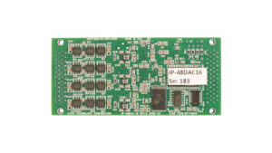
| Mechanical Interface | Switched Mezzanine Card (XMC) Interface confirming to ANSI/VITA 42.0-2008 (Auxiliary Standard) Standard single-width (149mm x 74mm) | |||||||||
| Electrical Interface | PCI Express x4 Link (Base Specification 2.1) compliant interface conforming to ANSI/VITA 42.3-2006 (PCI Express Protocol Layer Standard) | |||||||||
| PCI Express Switch | PI7C9X2G312GP (Pericom) | |||||||||
| PCI Express to PCI Bridge | XIO2001 (Texas Instruments) | |||||||||
| User configurable FPGA | TXMC639-10R: XC7K160T-2FBG676I (AMD) TXMC639-11R: XC7K325T-2FBG676I (AMD) | |||||||||
| SPI-Flash | MT25QL128 (Micron) 128 Mbit (contains TXMC639 FPGA BRD) or compatible; +3.3 V supply voltage | |||||||||
| DDR3 RAM | 2x MT41K256M16TW-107 (Micron) 256Meg x 32 bit | |||||||||
| Board Configuration Controller | LCMXO2-7000HC (Lattice) | |||||||||
| ADC | LTC2320 -16 (Analog Devices) | |||||||||
| DAC | AD5547BRUZ (Analog Devices) | |||||||||
| A/D Channels | TXMC639-10R: 8 Differential 16bit A/D Channels TXMC639-11R: 16 Differential 16bit A/D Channels Input Configuration per BCC Device: Input Voltage Ranges: Differental : ±20.57 V, ±10.28 V or ±5.14 V (Single-Ended: ±10.28 V, ±5.14 V or ±2.57 V) All analog inputs are connected via an impedance converter and a second operation amplifier for level adjustment and filtering to the differential ADC inputs. The -3 dB limit of this input stage is at approx. 8MHz | |||||||||
| D/A Channels | TXMC639-10R: 4 Single-Ended 16 Bit D/A Channels TXMC639-11R: 8 Single-Ended 16 Bit D/A Channels Output range configurable per D/A channel. Maximum single-ended Output Voltage – Vout: ±10 V Maximum Output Drive Current for each Output: 10 mA Maximum Capacitive Load for each Output: 1000 pF Typical Settling Time for a 10 mA / 1000 pF: < 1 µs | |||||||||
| Digital Front I/O Channels | 32 digital I/O Lines
| |||||||||
| Digital Rear I/O Channels | 64 direct FPGA I/O lines to P14 Rear I/O connector
4 MGT line to P16 Rear I/O connector
| |||||||||
| Front I/O | Front I/O Samtec – ERF8_050_01_L_D_RA_L_TR | |||||||||
| P14 Rear I/O | 64 pin Mezzanine Connector (Molex 71436-2864 or compatible) | |||||||||
| P16 Rear I/O | 114 pin Mezzanine Connector (Samtec – ASP-105885-01) | |||||||||
| Power Requirements 1) | Depends on FPGA design With TXMC639 Board Reference Design / without external load
| |||||||||
| Temperature Range | Operating: – 40 °C to + 85 °C Storage: – 55 °C to + 125 °C | |||||||||
| MTBF 1) | 157 000 h to 161 000 h | |||||||||
| Humidity | 5% – 95% non-condensing | |||||||||
| Weight | 140 g |
1) depends on variant, for further details see User Manual
TXMC639-10R
| 8x Analog In, 4x Analog Out, XC7K160T-2FBG676 Kintex™ 7 FPGA AMD Kintex™ 7 FPGA (XC7K160T-2FBG676), 1GB DDR3, 8x Analog In, 4x Analog Out, 32x digital Front I/O, 64x direct FPGA Rear I/O Lines and 4x MGTs Rear I/O |
TXMC639-11R
| 16x Analog In, 8x Analog Out, XC7K325T-2FBG676 Kintex™ 7 FPGA AMD Kintex™ 7 FPGA (XC7K325T-2FBG676), 1GB DDR3, 16x Analog In, 8x Analog Out, 32x digital Front I/O, 64x direct FPGA Rear I/O Lines and 4x MGTs Rear I/O |
SOFTWARE
Share this product
LinkedIn