- I/O Pins: Up to 48 I/O pins, independently programmable.
- Output Features: Direct read-back outputs, Open Collector VMOS that can sink up to 100mA at voltages up to 40V.
- Electrical Characteristics: Very low Ron (2Ω), low threshold of 1.6V max.
- Input/Output Range: Wide input range from 0V to 40V.
- Interrupt Features: Change of state detection can generate IP interrupts, selectable interrupts (from high to low or low to high).
- Additional Features: Integrated Altera logic, programmable time debouncing feature.

IP-DIO48-OC
Digital Input / Output Industry Pack 48 Channels I/O, Open Collector
- I/O Pins: Up to 48 I/O pins, independently programmable.
- Output Features: Direct read-back outputs, Open Collector VMOS that can sink up to 100mA at voltages up to 40V.
- Electrical Characteristics: Very low Ron (2Ω), low threshold of 1.6V max.
- Input/Output Range: Wide input range from 0V to 40V.
- Interrupt Features: Change of state detection can generate IP interrupts, selectable interrupts (from high to low or low to high).
- Additional Features: Integrated Altera logic, programmable time debouncing feature.
Share this product
LinkedIn
IP-DIO48-OC
Digital Input / Output Industry Pack 48 Channels I/O, Open Collector
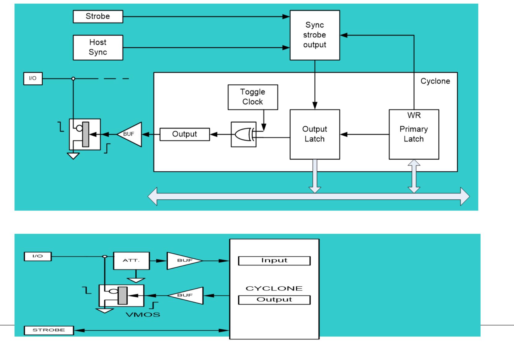
The IP-DIO48-OC is the perfect solution for control and monitor of switches and indicators or similar devices. For applications that need to work with a variety of input and output voltages ranging from 0-40 volts, the IP-DIO48-OC offers 48 independent channels on a single wide industry pack. Each of the channels of the IP-DIO48-OC can be configured individually as input / output.. – Single wide Industry Pack module – Programmable via IP bus – 8/32 Mhz IP clock support – Vita 4 compliant
Features
- Up to 48 I/O pins Independent programmable
- Direct read-back outputs
- Open Collector VMOS that can sink up to 100mA at voltage up to 40V.
- Very low Ron (2Ω)
- Change of state detection can generate IP Interrupt
- Integrated Altera logic
- Low Threshled 1.6 V Max
I/O Level
- Wide input range from 0V to 40V
- 48 Channels / Digital Input/ Outputs
- Time Debouncing feature, Programmable
- Selectable Interrupts (from High to Low or Low to High)
Programmable via
- IP Bus
IP interface
- 8/32 MHz clock
- 16 bit data
- Interrupts
Operating: Environmental
- Operating temperature
- Commercial: 0 to +55 °C
- Optional: -25°C to +80°C
- Non-operating: -40°C to 85 °C
- Airflow requirement: .5 CFM
- Humidity: 5 to 90% (non-cond.)
- Altitude: 0 to 10’000 ft
Mechanical: Environmental
- Size: Vita 4 Type 1 IP
Applications
- Process Control and Industrial Automation
- Precision Instrumentation
- Direct Digital Waveform Generation
- Software-Controlled Gain Adjustment
- Automatic Test Equipment
Programmable via
- IP Bus
IP interface
- 8/32 MHz clock
- 16 bit data
Operating: Environmental
- Operating temperature
- Commercial: 0 to +55 °C
- Optional: -25°C to +80°C
- Non-operating: -40°C to 85 °C
- Airflow requirement: 0.5 CFM
- Humidity: 5 to 90% (non-condensing)
- Altitude: 0 to 10,000 ft
Mechanical: Environmental
- Size: Vita 4 Type 1 IP 1.8″ x 3.9″
- Power: +5, +12, -12 volts
- Vibration: 0.5G RMS 20-2000 Hz rand
- Shock: 20 G, 11 ms, 1⁄2 sine
- Weight: tbd
- MTBF: >250,000 hours
- I/O Pins: Up to 48 I/O pins, independently programmable.
- Output Features: Direct read-back outputs, Open Collector VMOS that can sink up to 100mA at voltages up to 40V.
- Electrical Characteristics: Very low Ron (2Ω), low threshold of 1.6V max.
- Input/Output Range: Wide input range from 0V to 40V.
- Interrupt Features: Change of state detection can generate IP interrupts, selectable interrupts (from high to low or low to high).
- Additional Features: Integrated Altera logic, programmable time debouncing feature.
| Mechanical Interface | Switched Mezzanine Card (XMC) Interface confirming to ANSI/VITA 42.0-2008 (Auxiliary Standard) Standard single-width (149mm x 74mm) | |||||||||
| Electrical Interface | PCI Express x4 Link (Base Specification 2.1) compliant interface conforming to ANSI/VITA 42.3-2006 (PCI Express Protocol Layer Standard) | |||||||||
| PCI Express Switch | PI7C9X2G312GP (Pericom) | |||||||||
| PCI Express to PCI Bridge | XIO2001 (Texas Instruments) | |||||||||
| User configurable FPGA | TXMC639-10R: XC7K160T-2FBG676I (AMD) TXMC639-11R: XC7K325T-2FBG676I (AMD) | |||||||||
| SPI-Flash | MT25QL128 (Micron) 128 Mbit (contains TXMC639 FPGA BRD) or compatible; +3.3 V supply voltage | |||||||||
| DDR3 RAM | 2x MT41K256M16TW-107 (Micron) 256Meg x 32 bit | |||||||||
| Board Configuration Controller | LCMXO2-7000HC (Lattice) | |||||||||
| ADC | LTC2320 -16 (Analog Devices) | |||||||||
| DAC | AD5547BRUZ (Analog Devices) | |||||||||
| A/D Channels | TXMC639-10R: 8 Differential 16bit A/D Channels TXMC639-11R: 16 Differential 16bit A/D Channels Input Configuration per BCC Device: Input Voltage Ranges: Differental : ±20.57 V, ±10.28 V or ±5.14 V (Single-Ended: ±10.28 V, ±5.14 V or ±2.57 V) All analog inputs are connected via an impedance converter and a second operation amplifier for level adjustment and filtering to the differential ADC inputs. The -3 dB limit of this input stage is at approx. 8MHz | |||||||||
| D/A Channels | TXMC639-10R: 4 Single-Ended 16 Bit D/A Channels TXMC639-11R: 8 Single-Ended 16 Bit D/A Channels Output range configurable per D/A channel. Maximum single-ended Output Voltage – Vout: ±10 V Maximum Output Drive Current for each Output: 10 mA Maximum Capacitive Load for each Output: 1000 pF Typical Settling Time for a 10 mA / 1000 pF: < 1 µs | |||||||||
| Digital Front I/O Channels | 32 digital I/O Lines
| |||||||||
| Digital Rear I/O Channels | 64 direct FPGA I/O lines to P14 Rear I/O connector
4 MGT line to P16 Rear I/O connector
| |||||||||
| Front I/O | Front I/O Samtec – ERF8_050_01_L_D_RA_L_TR | |||||||||
| P14 Rear I/O | 64 pin Mezzanine Connector (Molex 71436-2864 or compatible) | |||||||||
| P16 Rear I/O | 114 pin Mezzanine Connector (Samtec – ASP-105885-01) | |||||||||
| Power Requirements 1) | Depends on FPGA design With TXMC639 Board Reference Design / without external load
| |||||||||
| Temperature Range | Operating: – 40 °C to + 85 °C Storage: – 55 °C to + 125 °C | |||||||||
| MTBF 1) | 157 000 h to 161 000 h | |||||||||
| Humidity | 5% – 95% non-condensing | |||||||||
| Weight | 140 g |
1) depends on variant, for further details see User Manual
TXMC639-10R
| 8x Analog In, 4x Analog Out, XC7K160T-2FBG676 Kintex™ 7 FPGA AMD Kintex™ 7 FPGA (XC7K160T-2FBG676), 1GB DDR3, 8x Analog In, 4x Analog Out, 32x digital Front I/O, 64x direct FPGA Rear I/O Lines and 4x MGTs Rear I/O |
TXMC639-11R
| 16x Analog In, 8x Analog Out, XC7K325T-2FBG676 Kintex™ 7 FPGA AMD Kintex™ 7 FPGA (XC7K325T-2FBG676), 1GB DDR3, 16x Analog In, 8x Analog Out, 32x digital Front I/O, 64x direct FPGA Rear I/O Lines and 4x MGTs Rear I/O |
SOFTWARE
Share this product
LinkedIn


