- Form Factor: Single-wide XMC (2.92” x 5.87”)
- MIL-STD-1553 Controller: 1 or 2 UTMC SUMMIT UT69151DX-GPC
- Modes: BC (Bus Controller), RT (Remote Terminal), BM (Bus Monitor)
- Transceivers & Transformers: On-chip transceivers, on-board transformers
- Stub Options: Long stub / Short stub
- Memory: 1 or 2 banks 128 Kbyte SRAM
- I/O: 1553 bus levels, TTL (5v) clock, front panel or rear I/O
- Interrupts: Supported
- Clock: Selectable Internal / external CLK
- Connectors: Optional front panel or rear I/O
- Options: MIL-STD-1553B, optional IRIG-B, VITA 42 compliant, 1 Lane PCIeXpress


XMC-1553-x
DUAL UTMC 1553 SUMMIT CONTROLLER BUS CONTROLLER, REMOTE TERMINAL, BUS MONITOR MODES
- Form Factor: Single-wide XMC (2.92” x 5.87”)
- MIL-STD-1553 Controller: 1 or 2 UTMC SUMMIT UT69151DX-GPC
- Modes: BC (Bus Controller), RT (Remote Terminal), BM (Bus Monitor)
- Transceivers & Transformers: On-chip transceivers, on-board transformers
- Stub Options: Long stub / Short stub
- Memory: 1 or 2 banks 128 Kbyte SRAM
- I/O: 1553 bus levels, TTL (5v) clock, front panel or rear I/O
- Interrupts: Supported
- Clock: Selectable Internal / external CLK
- Connectors: Optional front panel or rear I/O
- Options: MIL-STD-1553B, optional IRIG-B, VITA 42 compliant, 1 Lane PCIeXpress
Share this product
LinkedIn
XMC-1553-x
DUAL UTMC 1553 SUMMIT CONTROLLER BUS CONTROLLER, REMOTE TERMINAL, BUS MONITOR MODES
MIL-STD-1553B, optional IRIG-B, VITA 42 compliant, 1 Lane PCIe, options include temperature ranges of 0 to +70 degrees and -40 to +85 degrees, conformal coating, 128 Kbyte SRAM per channel, BC/RT/M modes, separate logic for the XMC interface, two dual redundant channels (Channel 1 A+B, Channel 2 A+B), selectable internal/external CLK, 78 ohm transformers, long/short stub, 5.0v or 3.3v VIO, low power, LED status, and available software includes ‘C’ libraries for Windows, Linux, and VxWorks.
Features
- 1 or 2 UTMC SUMMIT controllers
- UT69151DX-GPC
- BC / RT / BM modes
- On-chip transceivers
- On-board transformers
- Long stub or short stub configurations
Memory
- 1 or 2 banks of 128Kbytes SRAM
- Programmable via XMC Bus
XMC Interface
- 3.3V I/O, 5V tolerant bus interfaces
- Local bus clock rates at 66MHz
- Compliant with PCIe Specification r1.0a
- PCIMG 1.x
- Direct slave data transfers
- DMA
I/O
- 1553 bus levels
- TTL (5v) clock
- Front panel or rear I/O
MIL-STD-1553
- Commercial temperature range: 0 to +70 °C
- Optional temperature range: -40°C to +80°C
- Airflow requirement: 0.5 CFM
- Humidity: 5 to 90% (non-cond.)
- Altitude: up to 20,000 ft
Mechanical Specifications
- Single wide XMC size: 2.92” x 5.87”
- Power consumption: 1.5 watts
- Front panel I/O
- Vibration resistance: 0.5G RMS (20-2000 Hz)
- Shock resistance: 20 G, 11 ms, ½ sine
- Weight: To be determined
- MTBF: >250,000 hours
Part Number : XMC-1553-1- (1) MIL-1553, BC/RT/M, UTMC SUMMIT, No IRIG-B
Part Number : XMC-1553-2- (2) MIL-1553, BC/RT/M, UTMC SUMMIT, No IRIG-B
-
- C – 0ºC to +70 ºC Temperature rating
- I – -40ºC to +85 ºC Temperature rating
- FP Front Panel Access Only
- RP Rear Panel Access Only
- –IRIG IRIG-B Option
Optional Accessories:
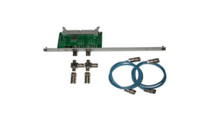
- Part Number : EngKit-1553-micro 2 T’s, 2 Terminators, 1 16 inch cables
- Part Number : CBL-1553-micro Standard-Standard 16 inch 1553 cable
- Form Factor: Single-wide XMC (2.92” x 5.87”)
- MIL-STD-1553 Controller: 1 or 2 UTMC SUMMIT UT69151DX-GPC
- Modes: BC (Bus Controller), RT (Remote Terminal), BM (Bus Monitor)
- Transceivers & Transformers: On-chip transceivers, on-board transformers
- Stub Options: Long stub / Short stub
- Memory: 1 or 2 banks 128 Kbyte SRAM
- I/O: 1553 bus levels, TTL (5v) clock, front panel or rear I/O
- Interrupts: Supported
- Clock: Selectable Internal / external CLK
- Connectors: Optional front panel or rear I/O
- Options: MIL-STD-1553B, optional IRIG-B, VITA 42 compliant, 1 Lane PCIeXpress
| Mechanical Interface | Switched Mezzanine Card (XMC) Interface confirming to ANSI/VITA 42.0-2008 (Auxiliary Standard) Standard single-width (149mm x 74mm) | |||||||||
| Electrical Interface | PCI Express x4 Link (Base Specification 2.1) compliant interface conforming to ANSI/VITA 42.3-2006 (PCI Express Protocol Layer Standard) | |||||||||
| PCI Express Switch | PI7C9X2G312GP (Pericom) | |||||||||
| PCI Express to PCI Bridge | XIO2001 (Texas Instruments) | |||||||||
| User configurable FPGA | TXMC639-10R: XC7K160T-2FBG676I (AMD) TXMC639-11R: XC7K325T-2FBG676I (AMD) | |||||||||
| SPI-Flash | MT25QL128 (Micron) 128 Mbit (contains TXMC639 FPGA BRD) or compatible; +3.3 V supply voltage | |||||||||
| DDR3 RAM | 2x MT41K256M16TW-107 (Micron) 256Meg x 32 bit | |||||||||
| Board Configuration Controller | LCMXO2-7000HC (Lattice) | |||||||||
| ADC | LTC2320 -16 (Analog Devices) | |||||||||
| DAC | AD5547BRUZ (Analog Devices) | |||||||||
| A/D Channels | TXMC639-10R: 8 Differential 16bit A/D Channels TXMC639-11R: 16 Differential 16bit A/D Channels Input Configuration per BCC Device: Input Voltage Ranges: Differental : ±20.57 V, ±10.28 V or ±5.14 V (Single-Ended: ±10.28 V, ±5.14 V or ±2.57 V) All analog inputs are connected via an impedance converter and a second operation amplifier for level adjustment and filtering to the differential ADC inputs. The -3 dB limit of this input stage is at approx. 8MHz | |||||||||
| D/A Channels | TXMC639-10R: 4 Single-Ended 16 Bit D/A Channels TXMC639-11R: 8 Single-Ended 16 Bit D/A Channels Output range configurable per D/A channel. Maximum single-ended Output Voltage – Vout: ±10 V Maximum Output Drive Current for each Output: 10 mA Maximum Capacitive Load for each Output: 1000 pF Typical Settling Time for a 10 mA / 1000 pF: < 1 µs | |||||||||
| Digital Front I/O Channels | 32 digital I/O Lines
| |||||||||
| Digital Rear I/O Channels | 64 direct FPGA I/O lines to P14 Rear I/O connector
4 MGT line to P16 Rear I/O connector
| |||||||||
| Front I/O | Front I/O Samtec – ERF8_050_01_L_D_RA_L_TR | |||||||||
| P14 Rear I/O | 64 pin Mezzanine Connector (Molex 71436-2864 or compatible) | |||||||||
| P16 Rear I/O | 114 pin Mezzanine Connector (Samtec – ASP-105885-01) | |||||||||
| Power Requirements 1) | Depends on FPGA design With TXMC639 Board Reference Design / without external load
| |||||||||
| Temperature Range | Operating: – 40 °C to + 85 °C Storage: – 55 °C to + 125 °C | |||||||||
| MTBF 1) | 157 000 h to 161 000 h | |||||||||
| Humidity | 5% – 95% non-condensing | |||||||||
| Weight | 140 g |
1) depends on variant, for further details see User Manual
TXMC639-10R
| 8x Analog In, 4x Analog Out, XC7K160T-2FBG676 Kintex™ 7 FPGA AMD Kintex™ 7 FPGA (XC7K160T-2FBG676), 1GB DDR3, 8x Analog In, 4x Analog Out, 32x digital Front I/O, 64x direct FPGA Rear I/O Lines and 4x MGTs Rear I/O |
TXMC639-11R
| 16x Analog In, 8x Analog Out, XC7K325T-2FBG676 Kintex™ 7 FPGA AMD Kintex™ 7 FPGA (XC7K325T-2FBG676), 1GB DDR3, 16x Analog In, 8x Analog Out, 32x digital Front I/O, 64x direct FPGA Rear I/O Lines and 4x MGTs Rear I/O |
SOFTWARE
Share this product
LinkedIn