- Single wide industry pack board format
- Altera FPGA EP2C20 or EP2C50
- Up to 24xRS485 or RS422 driver/receiver (LTC2861) or TTL input/output lines
- Each line can be separately selected as input or output
- Programmable in groups of 4 I/O
- 100Ω terminating resistor or no resistor for RS485/RS422 I/O, resistor software selectable using LTC2861 switch
- Up to 512K x 8 x 2 dual-ported SRAM
- MAX 3128 timing device for IP bus, DPR bus, and FLEX device access
- 8 or 32 MHz clock
- Optional user clock on board running at different speeds than IP bus
- 2 interrupts and 2 slave DMA IP bus lines
- FPGA programmable through JTAG header, onboard serial EPROM, or through IP bus
- VITA 4 compliant


IP-CYCLONE II-PIO
IP Cyclone FPGA with RS485/RS422/TTL Parallel I/O
- Single wide industry pack board format
- Altera FPGA EP2C20 or EP2C50
- Up to 24xRS485 or RS422 driver/receiver (LTC2861) or TTL input/output lines
- Each line can be separately selected as input or output
- Programmable in groups of 4 I/O
- 100Ω terminating resistor or no resistor for RS485/RS422 I/O, resistor software selectable using LTC2861 switch
- Up to 512K x 8 x 2 dual-ported SRAM
- MAX 3128 timing device for IP bus, DPR bus, and FLEX device access
- 8 or 32 MHz clock
- Optional user clock on board running at different speeds than IP bus
- 2 interrupts and 2 slave DMA IP bus lines
- FPGA programmable through JTAG header, onboard serial EPROM, or through IP bus
- VITA 4 compliant
Share this product
LinkedIn
IP-CYCLONE II-PIO
IP Cyclone FPGA with RS485/RS422/TTL Parallel I/O
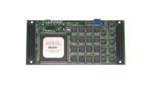
The IP-CYCLONEII-PIO module is an IndustryPack mezzanine card featuring an Altera Cyclone II embedded programmable FPGA, available in two sizes: EP2C20 and EP2C50. It supports dual-ported SRAM accessible by both the IP bus and the Cyclone FPGA, allowing for flexible data management. The I/O capabilities include up to 24 pairs of RS-485/RS-422 or 48 TTL lines, configurable in groups of 4. This module is suitable for applications requiring RS-485/RS-422 bus I/O interfaces or TTL I/O subsystems for monitoring and controlling digital functions.
FPGA Programming
- Programmable through Blaster interface for quick design turnaround
- Local serial EPROM for local programming
- Downloadable via IP bus for secure applications
LTC2861 – 20Mbps RS485 Transceivers Features
- 20 Mbps Max Data Rate
- ESD protection: ±15kV HBM
- High Input Impedance Supports 256 Nodes
- 250kbps Low-EMI Mode Full duplex
- Failsafe Receiver Operation Over Entire Common Mode Range
- Current Limited Drivers and Thermal Shutdown
- Delayed Micropower Shutdown (5μA Max)
- Low Operating Current (900μA Max in Receive Mode)
I/O Features (TTL mode)
- 24 pair RS-422/485 or 48 TTL or combination
- High Input Impedance-Supports 256 nodes
- Software selectable Half-Full Duplex
- Enhanced ESD protection (±15 KV)
- Logic-Selectable 120Ω Termination Resistor
Industry Pack Specifications
- Meets ANSI/VITA 4-1995
- 8/32 MHz synchronous operation
- Supports ID, 128 byte I/O, interrupt, & 8 Mbyte memory spaces
- 2 Interrupts per module
- Two passive DMA channels possible
- Hardware self timed per IP module
- Triggered via system reset and software control
- Jumper or software time-out function
- 5, +/-12 volt reset-able fuse per IP
Mechanical: Environmental
- Size: VITA 4 compliant 1.8″ x 3.9″ or 46 mm x 99 mm
- Power: 1.0 watt
- Vibration: 0.5G, 20-2000 Hz rand
- Shock: 20G, 11 msec, 1⁄2 sine
- Weight: 3 ounces
- MTBF: >250,000 hours
Operating Environment
- Operating temperature
- Commercial: 0 to +70°C
- Industrial: -40°C to +85°C
- Airflow requirement: 5 CFM
- Humidity: 5 to 90% (non-condensing)
- Altitude: 0 to 10,000 feet
Ordering Information:
- Part Number : Commercial: 0 to +70 oC
- IP-Cyclone II-C20 – PIO RS-485/422 ALTERA EP2C20 Industry Pack module
- IP-Cyclone II-C50 – PIO RS-485/422 ALTERA EP2C50 Industry Pack module
- Industrial: -40 oC to +85 oC
- IP-Cyclone II-C20 – PIO-I RS-485/422 ALTERA EP2C20 Industry Pack module
- IP-Cyclone II-C50 – PIO -I RS-485/422 ALTERA EP2C50 Industry Pack module
Optional Accessories
- Part Number : TB-50-HDR 50 pin terminal block and 1 meter flat ribbon cable
- Part Number : CBL-50-HDR 50 pin, 1 meter flat ribbon cable, IDC header connector
- Single wide industry pack board format
- Altera FPGA EP2C20 or EP2C50
- Up to 24xRS485 or RS422 driver/receiver (LTC2861) or TTL input/output lines
- Each line can be separately selected as input or output
- Programmable in groups of 4 I/O
- 100Ω terminating resistor or no resistor for RS485/RS422 I/O, resistor software selectable using LTC2861 switch
- Up to 512K x 8 x 2 dual-ported SRAM
- MAX 3128 timing device for IP bus, DPR bus, and FLEX device access
- 8 or 32 MHz clock
- Optional user clock on board running at different speeds than IP bus
- 2 interrupts and 2 slave DMA IP bus lines
- FPGA programmable through JTAG header, onboard serial EPROM, or through IP bus
- VITA 4 compliant
| Mechanical Interface | Switched Mezzanine Card (XMC) Interface confirming to ANSI/VITA 42.0-2008 (Auxiliary Standard) Standard single-width (149mm x 74mm) | |||||||||
| Electrical Interface | PCI Express x4 Link (Base Specification 2.1) compliant interface conforming to ANSI/VITA 42.3-2006 (PCI Express Protocol Layer Standard) | |||||||||
| PCI Express Switch | PI7C9X2G312GP (Pericom) | |||||||||
| PCI Express to PCI Bridge | XIO2001 (Texas Instruments) | |||||||||
| User configurable FPGA | TXMC639-10R: XC7K160T-2FBG676I (AMD) TXMC639-11R: XC7K325T-2FBG676I (AMD) | |||||||||
| SPI-Flash | MT25QL128 (Micron) 128 Mbit (contains TXMC639 FPGA BRD) or compatible; +3.3 V supply voltage | |||||||||
| DDR3 RAM | 2x MT41K256M16TW-107 (Micron) 256Meg x 32 bit | |||||||||
| Board Configuration Controller | LCMXO2-7000HC (Lattice) | |||||||||
| ADC | LTC2320 -16 (Analog Devices) | |||||||||
| DAC | AD5547BRUZ (Analog Devices) | |||||||||
| A/D Channels | TXMC639-10R: 8 Differential 16bit A/D Channels TXMC639-11R: 16 Differential 16bit A/D Channels Input Configuration per BCC Device: Input Voltage Ranges: Differental : ±20.57 V, ±10.28 V or ±5.14 V (Single-Ended: ±10.28 V, ±5.14 V or ±2.57 V) All analog inputs are connected via an impedance converter and a second operation amplifier for level adjustment and filtering to the differential ADC inputs. The -3 dB limit of this input stage is at approx. 8MHz | |||||||||
| D/A Channels | TXMC639-10R: 4 Single-Ended 16 Bit D/A Channels TXMC639-11R: 8 Single-Ended 16 Bit D/A Channels Output range configurable per D/A channel. Maximum single-ended Output Voltage – Vout: ±10 V Maximum Output Drive Current for each Output: 10 mA Maximum Capacitive Load for each Output: 1000 pF Typical Settling Time for a 10 mA / 1000 pF: < 1 µs | |||||||||
| Digital Front I/O Channels | 32 digital I/O Lines
| |||||||||
| Digital Rear I/O Channels | 64 direct FPGA I/O lines to P14 Rear I/O connector
4 MGT line to P16 Rear I/O connector
| |||||||||
| Front I/O | Front I/O Samtec – ERF8_050_01_L_D_RA_L_TR | |||||||||
| P14 Rear I/O | 64 pin Mezzanine Connector (Molex 71436-2864 or compatible) | |||||||||
| P16 Rear I/O | 114 pin Mezzanine Connector (Samtec – ASP-105885-01) | |||||||||
| Power Requirements 1) | Depends on FPGA design With TXMC639 Board Reference Design / without external load
| |||||||||
| Temperature Range | Operating: – 40 °C to + 85 °C Storage: – 55 °C to + 125 °C | |||||||||
| MTBF 1) | 157 000 h to 161 000 h | |||||||||
| Humidity | 5% – 95% non-condensing | |||||||||
| Weight | 140 g |
1) depends on variant, for further details see User Manual
TXMC639-10R
| 8x Analog In, 4x Analog Out, XC7K160T-2FBG676 Kintex™ 7 FPGA AMD Kintex™ 7 FPGA (XC7K160T-2FBG676), 1GB DDR3, 8x Analog In, 4x Analog Out, 32x digital Front I/O, 64x direct FPGA Rear I/O Lines and 4x MGTs Rear I/O |
TXMC639-11R
| 16x Analog In, 8x Analog Out, XC7K325T-2FBG676 Kintex™ 7 FPGA AMD Kintex™ 7 FPGA (XC7K325T-2FBG676), 1GB DDR3, 16x Analog In, 8x Analog Out, 32x digital Front I/O, 64x direct FPGA Rear I/O Lines and 4x MGTs Rear I/O |
SOFTWARE
Share this product
LinkedIn