- Single-wide Industry Pack board
- Altera FPGA 10K50E, 10K100E, or 10K130E
- Up to 24 LVDS driver/receiver pairs (SN65MLVD204AD) or 48 TTL I/O lines
- Each line can be separately selected as input or output in TTL mode
- Programmable in groups of 4 I/O
- 100Ω terminating resistor or no resistor for LVDS I/O, resistor software selectable using MAX335 switch
- Up to 512K x 8 x 2 dual-ported SRAM
- EPM7160 timing device for IP bus, DPR bus, and FLEX device access


IP-10K50E-LVDS
IP ALTERA 10K50E with LVDS Parallel I/O
- Single-wide Industry Pack board
- Altera FPGA 10K50E, 10K100E, or 10K130E
- Up to 24 LVDS driver/receiver pairs (SN65MLVD204AD) or 48 TTL I/O lines
- Each line can be separately selected as input or output in TTL mode
- Programmable in groups of 4 I/O
- 100Ω terminating resistor or no resistor for LVDS I/O, resistor software selectable using MAX335 switch
- Up to 512K x 8 x 2 dual-ported SRAM
- EPM7160 timing device for IP bus, DPR bus, and FLEX device access
Share this product
LinkedIn
IP-10K50E-LVDS
IP ALTERA 10K50E with LVDS Parallel I/O
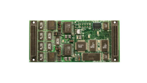
The IP-1OK50E-PIO module is an IP mezzanine card that is populated with an Altera FLEX 10Kxxx embedded programmable FPGA. Three different sized FPGAs can be selected. A dual-ported SRAM can be accessed by either some form of CPU/DSP on the IP bus side and/or the FLEX 10Kxxx FPGA. The I/O can be either LVDS or TTL in groups of 4 I/O.
All Features:
- Single-wide Industry Pack board
- Altera FPGA 10K50E, 10K100E, or 10K130E
- Up to 24 LVDS driver/receiver pairs (SN65MLVD204AD) or 48 TTL I/O lines
- Each line can be separately selected as input or output in TTL mode
- Programmable in groups of 4 I/O
- 100Ω terminating resistor or no resistor for LVDS I/O, resistor software selectable using MAX335 switch
- Up to 512K x 8 x 2 dual-ported SRAM
- EPM7160 timing device for IP bus, DPR bus, and FLEX device access
- 8 or 32 MHz clock
- Optional user clock on board running at different speed than IP bus
- 2 interrupts and 2 slave DMA IP bus lines
- FPGA programmable through bit/byte Blaster header, onboard serial EPROM, or through IP bus
- VITA 4 compliant
Available Software Drivers:
The customer must have an Altera development tool to implement their own FPGA design. The IP module can be used as a stand-alone module.
The FPGA’s program can be downloaded in one of three ways:
-
- Bit/byte Blaster header connector connected directly to the FPGA
- Local serial EPROM
- Through the IP bus
Applications:
The IP-10K50E-PIO can be used as an LVDS bus I/O interface for parallel and/or serial communications between carrier systems or simply as a TTL I/O subsystem for monitoring and/or controlling digitally oriented functions.
The FPGA can be programmed through the Blaster interface for quick design turnaround. The local serial EPROM can be used for local programming. The FPGA can also be programmed by downloading the entire program into the FPGA from the IP bus for applications that require complete security.
SN65MLVD204AD LVDS Transceiver I/O Features (LVDS Mode):
-
-
- Signaling rates up to 100 Mbps, clock frequencies up to 50 MHz
- Type 2 receivers provide an offset (100 mV) threshold to detect open-circuit and idle-bus conditions
- Meets or exceeds the M-LVDS standard TIA/EIA-899 for multipoint data interchange
- Controlled driver output voltage transition times for improved signal quality
- -1 V to 3.4 V common-mode voltage range allows data transfer with 2 V of ground noise
- Differential output voltage magnitude = 650 mV max
- Positive going differential input voltage threshold = 150 mV
- Negative going differential input voltage threshold = 50 mV min
- Differential input voltage hysteresis = 0 mV
-
FLEX I/O Features (TTL Mode):
-
-
- Low input voltage max = 0.8 VDC
- High input voltage min = 2.0 VDC
- Low output voltage max = 0.45 VDC
- High output voltage min = 2.4 VDC
- Max output current = 25 mA at Vcc = 5.0 VDC
-
Industry Pack Specifications:
-
-
- Meets ANSI/VITA 4-1995
- 8/32 MHz synchronous operation
- Supports ID, 128-byte I/O, interrupt, & 8 Mbyte memory spaces
- 2 interrupts per module
- Two passive DMA channels are possible
- Hardware self-timed per IP module
- Triggered via system reset and software control
- Jumper or software time-out function
- 5, +/-12 volt reset-able fuse per IP
-
Mechanical & Environmental:
-
-
- Size – VITA 4 compatible 1.8” x 3.9” (46 mm x 99 mm)
- Power – 1.0 watt
- Vibration – 0.5G, 20-2000 Hz random
- Shock – 20G, 11 msec, ½ sine
- Weight – TBD
- MTBF – >250,000 hours
-
Operating Environment:
-
- Operating temperature:
- Commercial: 0 to +70 ºC
- Optional: -25 ºC to +80 ºC
- Non-operating: -40 ºC to +85 ºC
- Airflow requirement – 5 CFM
- Humidity – 5 to 90% (non-condensing)
- Altitude – 0 to 10,000 feet
- Operating temperature:
Part Numbers:
-
- IP-Altera-10K50E-LVDS:
LVDS ALTERA 10K50E Industry Pack module - IP-Altera-10K100E-LVDS:
LVDS ALTERA 10K100E Industry Pack module
- IP-Altera-10K130E-LVDS:
LVDS ALTERA 10K130E Industry Pack module
- IP-Altera-10K50E-LVDS:
Optional Accessories:
- Part Number: TB-50-HDR
50 pin terminal block and 1 meter flat ribbon cable - Part Number: CBL-50-HDR
50 pin, 1 meter flat ribbon cable, IDC header connector
- Single-wide Industry Pack board
- Altera FPGA 10K50E, 10K100E, or 10K130E
- Up to 24 LVDS driver/receiver pairs (SN65MLVD204AD) or 48 TTL I/O lines
- Each line can be separately selected as input or output in TTL mode
- Programmable in groups of 4 I/O
- 100Ω terminating resistor or no resistor for LVDS I/O, resistor software selectable using MAX335 switch
- Up to 512K x 8 x 2 dual-ported SRAM
- EPM7160 timing device for IP bus, DPR bus, and FLEX device access
| Mechanical Interface | Switched Mezzanine Card (XMC) Interface confirming to ANSI/VITA 42.0-2008 (Auxiliary Standard) Standard single-width (149mm x 74mm) | |||||||||
| Electrical Interface | PCI Express x4 Link (Base Specification 2.1) compliant interface conforming to ANSI/VITA 42.3-2006 (PCI Express Protocol Layer Standard) | |||||||||
| PCI Express Switch | PI7C9X2G312GP (Pericom) | |||||||||
| PCI Express to PCI Bridge | XIO2001 (Texas Instruments) | |||||||||
| User configurable FPGA | TXMC639-10R: XC7K160T-2FBG676I (AMD) TXMC639-11R: XC7K325T-2FBG676I (AMD) | |||||||||
| SPI-Flash | MT25QL128 (Micron) 128 Mbit (contains TXMC639 FPGA BRD) or compatible; +3.3 V supply voltage | |||||||||
| DDR3 RAM | 2x MT41K256M16TW-107 (Micron) 256Meg x 32 bit | |||||||||
| Board Configuration Controller | LCMXO2-7000HC (Lattice) | |||||||||
| ADC | LTC2320 -16 (Analog Devices) | |||||||||
| DAC | AD5547BRUZ (Analog Devices) | |||||||||
| A/D Channels | TXMC639-10R: 8 Differential 16bit A/D Channels TXMC639-11R: 16 Differential 16bit A/D Channels Input Configuration per BCC Device: Input Voltage Ranges: Differental : ±20.57 V, ±10.28 V or ±5.14 V (Single-Ended: ±10.28 V, ±5.14 V or ±2.57 V) All analog inputs are connected via an impedance converter and a second operation amplifier for level adjustment and filtering to the differential ADC inputs. The -3 dB limit of this input stage is at approx. 8MHz | |||||||||
| D/A Channels | TXMC639-10R: 4 Single-Ended 16 Bit D/A Channels TXMC639-11R: 8 Single-Ended 16 Bit D/A Channels Output range configurable per D/A channel. Maximum single-ended Output Voltage – Vout: ±10 V Maximum Output Drive Current for each Output: 10 mA Maximum Capacitive Load for each Output: 1000 pF Typical Settling Time for a 10 mA / 1000 pF: < 1 µs | |||||||||
| Digital Front I/O Channels | 32 digital I/O Lines
| |||||||||
| Digital Rear I/O Channels | 64 direct FPGA I/O lines to P14 Rear I/O connector
4 MGT line to P16 Rear I/O connector
| |||||||||
| Front I/O | Front I/O Samtec – ERF8_050_01_L_D_RA_L_TR | |||||||||
| P14 Rear I/O | 64 pin Mezzanine Connector (Molex 71436-2864 or compatible) | |||||||||
| P16 Rear I/O | 114 pin Mezzanine Connector (Samtec – ASP-105885-01) | |||||||||
| Power Requirements 1) | Depends on FPGA design With TXMC639 Board Reference Design / without external load
| |||||||||
| Temperature Range | Operating: – 40 °C to + 85 °C Storage: – 55 °C to + 125 °C | |||||||||
| MTBF 1) | 157 000 h to 161 000 h | |||||||||
| Humidity | 5% – 95% non-condensing | |||||||||
| Weight | 140 g |
1) depends on variant, for further details see User Manual
TXMC639-10R
| 8x Analog In, 4x Analog Out, XC7K160T-2FBG676 Kintex™ 7 FPGA AMD Kintex™ 7 FPGA (XC7K160T-2FBG676), 1GB DDR3, 8x Analog In, 4x Analog Out, 32x digital Front I/O, 64x direct FPGA Rear I/O Lines and 4x MGTs Rear I/O |
TXMC639-11R
| 16x Analog In, 8x Analog Out, XC7K325T-2FBG676 Kintex™ 7 FPGA AMD Kintex™ 7 FPGA (XC7K325T-2FBG676), 1GB DDR3, 16x Analog In, 8x Analog Out, 32x digital Front I/O, 64x direct FPGA Rear I/O Lines and 4x MGTs Rear I/O |
SOFTWARE
Share this product
LinkedIn