- Configuration: 8 A/D modules with 8 differential A/D inputs
- Acquisition Time: 100Ksps
- Programmable Gain: 1, 2, 4, 8
- FIFO: 256Kx16 FIFO for burst mode or continuous sampling at lower throughput using control logic
- Trigger Modes: Pre-trigger and post-trigger acquisition
- Sampling Clock Sources: Internal divider (IPCLK/N), IPSTROBE, or External clock
- Trigger Event Sources: Write to IP register, IPSTROBE, or External trigger
- Clock: 32 MHz clock
- Interrupts and DMA: 2 interrupts and 2 slave DMA IP bus lines
- VITA Compliance: VITA 4 compliant
- EEPROM: 32 bytes used for board ID

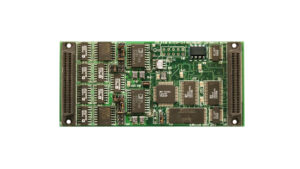
IP-AD8100
IP 16 bit A/D converter, 8 A/D modules with 256Kx16 FIFO
- Configuration: 8 A/D modules with 8 differential A/D inputs
- Acquisition Time: 100Ksps
- Programmable Gain: 1, 2, 4, 8
- FIFO: 256Kx16 FIFO for burst mode or continuous sampling at lower throughput using control logic
- Trigger Modes: Pre-trigger and post-trigger acquisition
- Sampling Clock Sources: Internal divider (IPCLK/N), IPSTROBE, or External clock
- Trigger Event Sources: Write to IP register, IPSTROBE, or External trigger
- Clock: 32 MHz clock
- Interrupts and DMA: 2 interrupts and 2 slave DMA IP bus lines
- VITA Compliance: VITA 4 compliant
- EEPROM: 32 bytes used for board ID
Share this product
LinkedIn
IP-AD8100
IP 16 bit A/D converter, 8 A/D modules with 256Kx16 FIFO
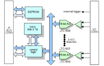
Block Diagram and Operational Overview The IP-AD100 has eight 16-bit A/D converters that run simultaneously at 100Ksps with front-end buffers that are fault protected. The A/D converters support bipolar voltage inputs, and include ±5VDC or ±10VDC The A/D converters operate continuously at the selected sampling rate. Results are either stored in the FIFO or discarded when appropriate. Only selected channels are saved into the FIFO, so that depth per channel is proportional to number of channels saved. The customer may desire to think of the IP module as similar to a Digital Storage Oscilloscope (DSO). A DSO can store and display several waveforms and can record signals prior to the trigger. The trigger point is completely configurable by reprogramming the FIFO’s programmable empty flag. A/D samples are acquired and stored into the 18 bit FIFO when acquisition has been started. Once the pre-trigger data has been acquired, triggering becomes active. Further, acquisition before the trigger that are seen will result in the earliest data being discarded at the same time new data is saved, thus maintaining the most recent data in the FIFO. Once the trigger event is seen, no more data is discarded from the FIFO, and acquisition proceeds until the FIFO is full. At this point, the acquisition stops, and the HOST can read the data from the IP. Interrupts can be sent to the HOST at Event and at acquisition finished. If desired, such as for a continuous acquisition, data can be read from the FIFO while acquisition is in progress, for continuous streaming. Unfortunately, it will not be possible to maintain a high sampling rate in this scenario due to the time constraints of the IP interface.
Applications:
This is a perfect solution for:
- Process control,
- Industrial control, or
- Precision instrumentation
Software Support:
The IP-AD8100 is supported under Windows NT /2000 by two sample programs, which are supplied with the IP in the board support package. Both examples are designed to work with an IP-type carrier from ALPHI, such as the PCI-4IPM.
One sample program, called SnapShot, fully exercises the IP module in pre- and post-trigger modes, and displays the data to the screen. Data can be stored to a file and can be reloaded in the program at a later time.
The second program, called DrawIpAdc, operates the IP in continuous mode, and displays the data to the screen.
Full source to both HOST DSP code and the applications are provided.
LTC1605 A/D Specifications:
- 16-bit, sampling A/D converter
- Fast throughput rate of 100Ksps
- On-chip clock
- Internal reference with external reference connection available for more accuracy
- Bipolar analog input voltage range: ±5VDC or ±10VDC (On Order selection)
- Integral linearity error ±2.0LSB max with no missing codes
- THD -102dB typical @ 1kHz, first 5 harmonics
- Full-scale bipolar error ±0.50% of FSR
- SNR 90dB at 10KHz typical
AD8251 Gain Amplifier Specifications:
- Programmable gains: 1, 2, 4, 8
- High CMRR: 98 dB (minimum), G =
- Low gain drift: 10 ppm/°C (maximum)
- Fast settling time: 785 ns to 0.001%
- High CMRR over frequency: 80 dB to 50kHz (minimum)
Industry Pack Specifications:
- Meets ANSI/VITA 4-1995
- 8/32 MHz synchronous operation
- Supports ID, 128 byte I/O, interrupt. & 8 Mbyte memory spaces
- 2 Interrupts per module
- Two passive DMA channels are possible.
- Hardware self timed per IP module
- Triggered via system reset and software control
- Jumper or software time-out function
- 5, +/-12 volt reset-able fuse per IP
Mechanical: Environmental:
- Size – VITA 4 compliant 1.8″ x 3.9″ or 46 mm x 99 mm
- Power – 1.0 watt
- Vibration – 0.5G, 20-2000 Hz rand
- Shock – 20G, 11 msec, 1⁄2 sine
- Weight – tbd
- MTBF – >250,000 hours
Operating Environment:
- Operating temperature Commercial: 0 to +70 oC Optional: -40 oC to +85 oC
- Non-operating: -45 oC to +90 oC
- Airflow requirement – 5 CFM
- Humidity – 5 to 90% (non-cond)
- Altitude – 0 to 10,000 feet
Part number:
IP-AD8100 8 channel, 16 bit, 100ksps A/D Industry Pack Module +/-5 Commercial (0 to +70 oC)
IP-AD8100 8 channel, 16 bit, 100ksps A/D Industry Pack Module – Industrial (0-40 oC to +85 oC)
- Configuration: 8 A/D modules with 8 differential A/D inputs
- Acquisition Time: 100Ksps
- Programmable Gain: 1, 2, 4, 8
- FIFO: 256Kx16 FIFO for burst mode or continuous sampling at lower throughput using control logic
- Trigger Modes: Pre-trigger and post-trigger acquisition
- Sampling Clock Sources: Internal divider (IPCLK/N), IPSTROBE, or External clock
- Trigger Event Sources: Write to IP register, IPSTROBE, or External trigger
- Clock: 32 MHz clock
- Interrupts and DMA: 2 interrupts and 2 slave DMA IP bus lines
- VITA Compliance: VITA 4 compliant
- EEPROM: 32 bytes used for board ID
| Mechanical Interface | Switched Mezzanine Card (XMC) Interface confirming to ANSI/VITA 42.0-2008 (Auxiliary Standard) Standard single-width (149mm x 74mm) | |||||||||
| Electrical Interface | PCI Express x4 Link (Base Specification 2.1) compliant interface conforming to ANSI/VITA 42.3-2006 (PCI Express Protocol Layer Standard) | |||||||||
| PCI Express Switch | PI7C9X2G312GP (Pericom) | |||||||||
| PCI Express to PCI Bridge | XIO2001 (Texas Instruments) | |||||||||
| User configurable FPGA | TXMC639-10R: XC7K160T-2FBG676I (AMD) TXMC639-11R: XC7K325T-2FBG676I (AMD) | |||||||||
| SPI-Flash | MT25QL128 (Micron) 128 Mbit (contains TXMC639 FPGA BRD) or compatible; +3.3 V supply voltage | |||||||||
| DDR3 RAM | 2x MT41K256M16TW-107 (Micron) 256Meg x 32 bit | |||||||||
| Board Configuration Controller | LCMXO2-7000HC (Lattice) | |||||||||
| ADC | LTC2320 -16 (Analog Devices) | |||||||||
| DAC | AD5547BRUZ (Analog Devices) | |||||||||
| A/D Channels | TXMC639-10R: 8 Differential 16bit A/D Channels TXMC639-11R: 16 Differential 16bit A/D Channels Input Configuration per BCC Device: Input Voltage Ranges: Differental : ±20.57 V, ±10.28 V or ±5.14 V (Single-Ended: ±10.28 V, ±5.14 V or ±2.57 V) All analog inputs are connected via an impedance converter and a second operation amplifier for level adjustment and filtering to the differential ADC inputs. The -3 dB limit of this input stage is at approx. 8MHz | |||||||||
| D/A Channels | TXMC639-10R: 4 Single-Ended 16 Bit D/A Channels TXMC639-11R: 8 Single-Ended 16 Bit D/A Channels Output range configurable per D/A channel. Maximum single-ended Output Voltage – Vout: ±10 V Maximum Output Drive Current for each Output: 10 mA Maximum Capacitive Load for each Output: 1000 pF Typical Settling Time for a 10 mA / 1000 pF: < 1 µs | |||||||||
| Digital Front I/O Channels | 32 digital I/O Lines
| |||||||||
| Digital Rear I/O Channels | 64 direct FPGA I/O lines to P14 Rear I/O connector
4 MGT line to P16 Rear I/O connector
| |||||||||
| Front I/O | Front I/O Samtec – ERF8_050_01_L_D_RA_L_TR | |||||||||
| P14 Rear I/O | 64 pin Mezzanine Connector (Molex 71436-2864 or compatible) | |||||||||
| P16 Rear I/O | 114 pin Mezzanine Connector (Samtec – ASP-105885-01) | |||||||||
| Power Requirements 1) | Depends on FPGA design With TXMC639 Board Reference Design / without external load
| |||||||||
| Temperature Range | Operating: – 40 °C to + 85 °C Storage: – 55 °C to + 125 °C | |||||||||
| MTBF 1) | 157 000 h to 161 000 h | |||||||||
| Humidity | 5% – 95% non-condensing | |||||||||
| Weight | 140 g |
1) depends on variant, for further details see User Manual
TXMC639-10R
| 8x Analog In, 4x Analog Out, XC7K160T-2FBG676 Kintex™ 7 FPGA AMD Kintex™ 7 FPGA (XC7K160T-2FBG676), 1GB DDR3, 8x Analog In, 4x Analog Out, 32x digital Front I/O, 64x direct FPGA Rear I/O Lines and 4x MGTs Rear I/O |
TXMC639-11R
| 16x Analog In, 8x Analog Out, XC7K325T-2FBG676 Kintex™ 7 FPGA AMD Kintex™ 7 FPGA (XC7K325T-2FBG676), 1GB DDR3, 16x Analog In, 8x Analog Out, 32x digital Front I/O, 64x direct FPGA Rear I/O Lines and 4x MGTs Rear I/O |
SOFTWARE
Share this product
LinkedIn