- M.2 PCI Express x1 lane interface
- M.2 3042 Key B & M
- Two dual redundant MIL-STD-1553 Total-AceXtreme® controllers (A/B channel)
- Multiprotocol support: MIL-STD-1553A/B STANAG-3838 and MIL-STD-1760
- 2MB RAM per Channel
- Programmable mode: Bus Controller, Remote Terminal with concurrent bus monitor
- IRIG-106 Chapter 10 monitor
- Emulate up to 31 RT addresses simultaneously
- Filter based on RT address, T/R bit, sub-address
- Transformer coupled


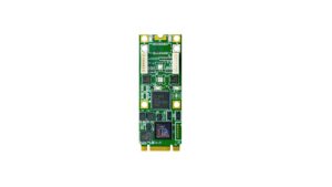
M.2-1553-2
Two Channels Dual Redundant 1553 Controller, Multiple RT Support
- M.2 PCI Express x1 lane interface
- M.2 3042 Key B & M
- Two dual redundant MIL-STD-1553 Total-AceXtreme® controllers (A/B channel)
- Multiprotocol support: MIL-STD-1553A/B STANAG-3838 and MIL-STD-1760
- 2MB RAM per Channel
- Programmable mode: Bus Controller, Remote Terminal with concurrent bus monitor
- IRIG-106 Chapter 10 monitor
- Emulate up to 31 RT addresses simultaneously
- Filter based on RT address, T/R bit, sub-address
- Transformer coupled
Share this product
LinkedIn
M.2-1553-2
Two Channels Dual Redundant 1553 Controller, Multiple RT Support
The M.2-1553-2 uses the DDC Total-AceXtreme communication device as its 1553 bus controller or remote terminal with concurrent bus monitor. The dual controller has a dual redundant channel with built-in transceivers and transformer. The controller has the capability to emulate up to 31 RT addresses simultaneously. The M.2-1553-2 in RT mode can filter on RT address, T/R, Subaddress. The M.2-1553-2 is offered in extended temperature. The board format is an M.2 30mm x 42mm.
- 1553 Capabilities
- Dual redundant MIL-STD-1553
- BC or Multi-RT with Concurrent Bus Monitor
- Supports MIL-STD-1553 A/B and MIL-STD-1760
- 2 MB (64K x 36) RAM
- 48-bit/100ns Time Stamp
- IRIG-106 Chapter 10 MT Support
- 1553 Bus Monitor (MT)
- IRIG-106 Chapter 10 compatibility
- Filter based on RT Address, T/R bit, Sub-Address
- Advanced bit-level error detection to isolate bus failures
- DMA engine for ultra-low CPU utilization
- 1553 Bus Remote Terminal (RT)
- Emulates up to 32 RT addresses simultaneously
- Multiple buffering techniques
- Programmable command illegalization
- Programmable busy by sub-address
- 1553 Bus Controller (BC)
- Streaming and minor/major frame scheduling of messages
- High- and low-priority asynchronous message insertion
- Modify messages or data while BC is running
- Applications
- Industrial and Military
- Test equipment supporting evaluation, simulation
- Monitoring and analysis
- Available Software Drivers
- Linux® drivers
- Windows® drivers
- VxWorks® drivers
- Mechanical
- Size: M.2 Module Key B & M (30mm x 42mm)
- Power: 240mA
- Front panel I/O
- Vibration: 0.5G, 20-2000Hz rand
- Shock: 20G, 11ms, ½ sine
- Weight: 10g (0.4oz)
- MTBF: >250,000 hours
- Operating Environment
- Operating temperature
- Commercial: 0 to +70ºC
- Industrial: -40ºC to +85ºC
- Non-operating: -50ºC to +90ºC
- Airflow requirement: .5CFM
- Humidity: 5 to 90% (non-cond)
- Altitude: 0 to 10,000 feet
- Operating temperature
M.2-1553-2
Two Channels Dual Redundant Controllers, Industrial Temp -40ºC to +85ºC
M.2-1553-1
One Channel Dual Redundant Controller, Industrial Temp -40ºC to +85ºC
Append -CC for Conformal Coat
Optional Accessories
CBL-M.2-1553-12 1 x Micro Connector to twin axial cable, 12in length
- M.2 PCI Express x1 lane interface
- M.2 3042 Key B & M
- Two dual redundant MIL-STD-1553 Total-AceXtreme® controllers (A/B channel)
- Multiprotocol support: MIL-STD-1553A/B STANAG-3838 and MIL-STD-1760
- 2MB RAM per Channel
- Programmable mode: Bus Controller, Remote Terminal with concurrent bus monitor
- IRIG-106 Chapter 10 monitor
- Emulate up to 31 RT addresses simultaneously
- Filter based on RT address, T/R bit, sub-address
- Transformer coupled
| Mechanical Interface | Switched Mezzanine Card (XMC) Interface confirming to ANSI/VITA 42.0-2008 (Auxiliary Standard) Standard single-width (149mm x 74mm) | |||||||||
| Electrical Interface | PCI Express x4 Link (Base Specification 2.1) compliant interface conforming to ANSI/VITA 42.3-2006 (PCI Express Protocol Layer Standard) | |||||||||
| PCI Express Switch | PI7C9X2G312GP (Pericom) | |||||||||
| PCI Express to PCI Bridge | XIO2001 (Texas Instruments) | |||||||||
| User configurable FPGA | TXMC639-10R: XC7K160T-2FBG676I (AMD) TXMC639-11R: XC7K325T-2FBG676I (AMD) | |||||||||
| SPI-Flash | MT25QL128 (Micron) 128 Mbit (contains TXMC639 FPGA BRD) or compatible; +3.3 V supply voltage | |||||||||
| DDR3 RAM | 2x MT41K256M16TW-107 (Micron) 256Meg x 32 bit | |||||||||
| Board Configuration Controller | LCMXO2-7000HC (Lattice) | |||||||||
| ADC | LTC2320 -16 (Analog Devices) | |||||||||
| DAC | AD5547BRUZ (Analog Devices) | |||||||||
| A/D Channels | TXMC639-10R: 8 Differential 16bit A/D Channels TXMC639-11R: 16 Differential 16bit A/D Channels Input Configuration per BCC Device: Input Voltage Ranges: Differental : ±20.57 V, ±10.28 V or ±5.14 V (Single-Ended: ±10.28 V, ±5.14 V or ±2.57 V) All analog inputs are connected via an impedance converter and a second operation amplifier for level adjustment and filtering to the differential ADC inputs. The -3 dB limit of this input stage is at approx. 8MHz | |||||||||
| D/A Channels | TXMC639-10R: 4 Single-Ended 16 Bit D/A Channels TXMC639-11R: 8 Single-Ended 16 Bit D/A Channels Output range configurable per D/A channel. Maximum single-ended Output Voltage – Vout: ±10 V Maximum Output Drive Current for each Output: 10 mA Maximum Capacitive Load for each Output: 1000 pF Typical Settling Time for a 10 mA / 1000 pF: < 1 µs | |||||||||
| Digital Front I/O Channels | 32 digital I/O Lines
| |||||||||
| Digital Rear I/O Channels | 64 direct FPGA I/O lines to P14 Rear I/O connector
4 MGT line to P16 Rear I/O connector
| |||||||||
| Front I/O | Front I/O Samtec – ERF8_050_01_L_D_RA_L_TR | |||||||||
| P14 Rear I/O | 64 pin Mezzanine Connector (Molex 71436-2864 or compatible) | |||||||||
| P16 Rear I/O | 114 pin Mezzanine Connector (Samtec – ASP-105885-01) | |||||||||
| Power Requirements 1) | Depends on FPGA design With TXMC639 Board Reference Design / without external load
| |||||||||
| Temperature Range | Operating: – 40 °C to + 85 °C Storage: – 55 °C to + 125 °C | |||||||||
| MTBF 1) | 157 000 h to 161 000 h | |||||||||
| Humidity | 5% – 95% non-condensing | |||||||||
| Weight | 140 g |
1) depends on variant, for further details see User Manual
TXMC639-10R
| 8x Analog In, 4x Analog Out, XC7K160T-2FBG676 Kintex™ 7 FPGA AMD Kintex™ 7 FPGA (XC7K160T-2FBG676), 1GB DDR3, 8x Analog In, 4x Analog Out, 32x digital Front I/O, 64x direct FPGA Rear I/O Lines and 4x MGTs Rear I/O |
TXMC639-11R
| 16x Analog In, 8x Analog Out, XC7K325T-2FBG676 Kintex™ 7 FPGA AMD Kintex™ 7 FPGA (XC7K325T-2FBG676), 1GB DDR3, 16x Analog In, 8x Analog Out, 32x digital Front I/O, 64x direct FPGA Rear I/O Lines and 4x MGTs Rear I/O |
SOFTWARE
Share this product
LinkedIn