- Based around the Texas Instruments floating-point Digital Signal Processor TMS320C6713B at 300 MHz
- Quad industry pack carrier configuration enabling a vast array of I/O possibilities creating a cost-effective solution of DSP and I/O
- Up to 192 I/O
- 1 X PCIexpress bus compatible
- Front panel I/O


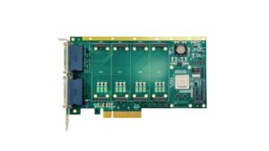
PCIe-6713-4IP
Intelligent PCIe Quad Industry Pack Carrier w/TM 320C6317B DSP
- Based around the Texas Instruments floating-point Digital Signal Processor TMS320C6713B at 300 MHz
- Quad industry pack carrier configuration enabling a vast array of I/O possibilities creating a cost-effective solution of DSP and I/O
- Up to 192 I/O
- 1 X PCIexpress bus compatible
- Front panel I/O
Share this product
LinkedIn
PCIe-6713-4IP
Intelligent PCIe Quad Industry Pack Carrier w/TM 320C6317B DSP
The board consists of private SDRAM and Flash memory attached to the 300 MHz TMS320C6713B DSP. An FPGA provides the timing and control. Peripherals include a serial port and connectors for IP mezzanine boards. Flash memory is available for downloading programs into a non-volatile memory. A PCIexpress bus connector provides the interface to the host computer. A serial port is available for debugging.
Available Software Drivers and Software Tools:
- C library dll’s
- Linux drivers
- Windows XP drivers
- VxWorks drivers
The TMS320C67x DSP generation is supported by the TI eXpressDSP™ set of industry development tools, including a highly optimizing C/C++ Compiler, the Code Composer Studio™ Integrated Development Environment (IDE), JTAG-based emulation, real-time debugging, and the DSP/BIOS™ kernel.
Applications:
For applications requiring low-cost, high-density I/O or unique combinations, the PCI6713B-4IP is the perfect solution. The Local DSP can be used to simply move data to and from the CPCI bus or provide pre-processing functions such as local PID controls, FFTs, digital filtering, etc. Custom application software can be downloaded to the DSP via the CompactPCI bus.
TMS320C6713 DSP Features:
- TMS320C6713B™ DSP @ 300 MHz
- 32/64 bit data word
- 8 32-bit instructions/cycle
- Up to 2400 MIPS/MFLOPS
- Advanced very long instruction word DSP core with 8 independent functional units – 2 ALUs (fixed point), 4 ALUs (floating/fixed point), and 2 multipliers (floating/fixed point)
- L1/L2 memory architecture: 4K byte L1P program cache, 4K byte L1D data cache (2-way), 256K byte L2 memory total with 64K-Byte L2 Unified Cache/Mapped RAM, and 192K-Byte Additional L2 Mapped RAM
- Load-store architecture with 32 32-bit general-purpose registers
- Native instructions for IEEE 754 single and double precision operations
- 32-bit external memory interface with a glueless interface to SRAM, EPROM, Flash, SBSRAM, and SDRAM with 512 Mbyte total addressable external memory space
- Dual 32-bit general-purpose timers
- 16-channel EDMA ‘Enhanced DMA’
- Two inter-integrated circuit buses (I2C Bus)
- 16-bit Host-Port Interface (HPI)
- IEEE-1149.1 (JTAG) boundary scan compatible
PCIe Bus:
- PLX 8311 66MHz 32-bit
- X1 link 2.5Gpbs/Direction
- 3.3V I/O bus interfaces
- Zero wait state burst operation, with PCI bus bursts to 264 MB/sec and local bus bursts to 264 MB/sec
- 2 DMA channels
- Direct master data transfers
- Direct slave data transfers
PCI Bus Control:
- I2O r1.5 messaging unit
- 8 mailboxes and 32 doorbell registers
- PCI arbiter supports 7 external masters
- Host mode reset/interrupt
- Power management event generation support
- Serial EEPROM interface
- JTAG boundary scan
85C30 Specifications:
- 2 serial channels
- Up to 1Mbps using a 16MHz clock, synchronous mode
- 5, 6, 7, or 8 bits per character
- 1, 1½, or 2 stop bits
- Odd or even parity
- X1, x16, x32, or x64 clock modes
- Character-oriented synchronous capabilities
- SDLC/HLDC capabilities
- NRZ, NRZI, or FM encoding/decoding
- Each serial channel has an independent baud rate generator
- DPLL for clock recovery
Industry Pack Specifications:
- Meets ANSI/VITA 4-1995
- 8/32 MHz synchronous operation
- Supports ID, 128-byte I/O, interrupt, & 8 Mbyte memory spaces
- 2 Interrupts per module
- Two passive DMA channels are possible
- Hardware self-timed per IP module
- Triggered via system reset and software control
- Jumper or software time-out function
- 5, +/-12 volt reset-able fuse per IP
- 8/16 bit data on 3U board, 32 bit on 6U board
Operating Environment:
- Operating temperature: Commercial 0 to +70 ºC, Optional -25 ºC to +80 ºC
- Non-operating: -40 ºC to +85 ºC
- Airflow requirement – 5 CFM
- Humidity – 5 to 90% (non-cond)
- Altitude – 0 to 10,000 feet
Mechanical Environment:
- Size PCIexpress module: 312 mm x 111 mm
- Power – 1.5 watt
- Vibration – 0.5G, 20-2000 Hz rand
- Shock – 20G, 11 msec, ½ sine
- Weight – 4-5 ounces
Ordering Information:
- PCIe-6713B-4 IP
6U industry pack carrier with 320C6713B DSP
Optional Accessories:
- CBL-50-HRS
Cable - TB-50-HRS
Terminal block
Data Sheet – Link Here
- Based around the Texas Instruments floating-point Digital Signal Processor TMS320C6713B at 300 MHz
- Quad industry pack carrier configuration enabling a vast array of I/O possibilities creating a cost-effective solution of DSP and I/O
- Up to 192 I/O
- 1 X PCIexpress bus compatible
- Front panel I/O
| Mechanical Interface | Switched Mezzanine Card (XMC) Interface confirming to ANSI/VITA 42.0-2008 (Auxiliary Standard) Standard single-width (149mm x 74mm) | |||||||||
| Electrical Interface | PCI Express x4 Link (Base Specification 2.1) compliant interface conforming to ANSI/VITA 42.3-2006 (PCI Express Protocol Layer Standard) | |||||||||
| PCI Express Switch | PI7C9X2G312GP (Pericom) | |||||||||
| PCI Express to PCI Bridge | XIO2001 (Texas Instruments) | |||||||||
| User configurable FPGA | TXMC639-10R: XC7K160T-2FBG676I (AMD) TXMC639-11R: XC7K325T-2FBG676I (AMD) | |||||||||
| SPI-Flash | MT25QL128 (Micron) 128 Mbit (contains TXMC639 FPGA BRD) or compatible; +3.3 V supply voltage | |||||||||
| DDR3 RAM | 2x MT41K256M16TW-107 (Micron) 256Meg x 32 bit | |||||||||
| Board Configuration Controller | LCMXO2-7000HC (Lattice) | |||||||||
| ADC | LTC2320 -16 (Analog Devices) | |||||||||
| DAC | AD5547BRUZ (Analog Devices) | |||||||||
| A/D Channels | TXMC639-10R: 8 Differential 16bit A/D Channels TXMC639-11R: 16 Differential 16bit A/D Channels Input Configuration per BCC Device: Input Voltage Ranges: Differental : ±20.57 V, ±10.28 V or ±5.14 V (Single-Ended: ±10.28 V, ±5.14 V or ±2.57 V) All analog inputs are connected via an impedance converter and a second operation amplifier for level adjustment and filtering to the differential ADC inputs. The -3 dB limit of this input stage is at approx. 8MHz | |||||||||
| D/A Channels | TXMC639-10R: 4 Single-Ended 16 Bit D/A Channels TXMC639-11R: 8 Single-Ended 16 Bit D/A Channels Output range configurable per D/A channel. Maximum single-ended Output Voltage – Vout: ±10 V Maximum Output Drive Current for each Output: 10 mA Maximum Capacitive Load for each Output: 1000 pF Typical Settling Time for a 10 mA / 1000 pF: < 1 µs | |||||||||
| Digital Front I/O Channels | 32 digital I/O Lines
| |||||||||
| Digital Rear I/O Channels | 64 direct FPGA I/O lines to P14 Rear I/O connector
4 MGT line to P16 Rear I/O connector
| |||||||||
| Front I/O | Front I/O Samtec – ERF8_050_01_L_D_RA_L_TR | |||||||||
| P14 Rear I/O | 64 pin Mezzanine Connector (Molex 71436-2864 or compatible) | |||||||||
| P16 Rear I/O | 114 pin Mezzanine Connector (Samtec – ASP-105885-01) | |||||||||
| Power Requirements 1) | Depends on FPGA design With TXMC639 Board Reference Design / without external load
| |||||||||
| Temperature Range | Operating: – 40 °C to + 85 °C Storage: – 55 °C to + 125 °C | |||||||||
| MTBF 1) | 157 000 h to 161 000 h | |||||||||
| Humidity | 5% – 95% non-condensing | |||||||||
| Weight | 140 g |
1) depends on variant, for further details see User Manual
TXMC639-10R
| 8x Analog In, 4x Analog Out, XC7K160T-2FBG676 Kintex™ 7 FPGA AMD Kintex™ 7 FPGA (XC7K160T-2FBG676), 1GB DDR3, 8x Analog In, 4x Analog Out, 32x digital Front I/O, 64x direct FPGA Rear I/O Lines and 4x MGTs Rear I/O |
TXMC639-11R
| 16x Analog In, 8x Analog Out, XC7K325T-2FBG676 Kintex™ 7 FPGA AMD Kintex™ 7 FPGA (XC7K325T-2FBG676), 1GB DDR3, 16x Analog In, 8x Analog Out, 32x digital Front I/O, 64x direct FPGA Rear I/O Lines and 4x MGTs Rear I/O |
SOFTWARE
Share this product
LinkedIn