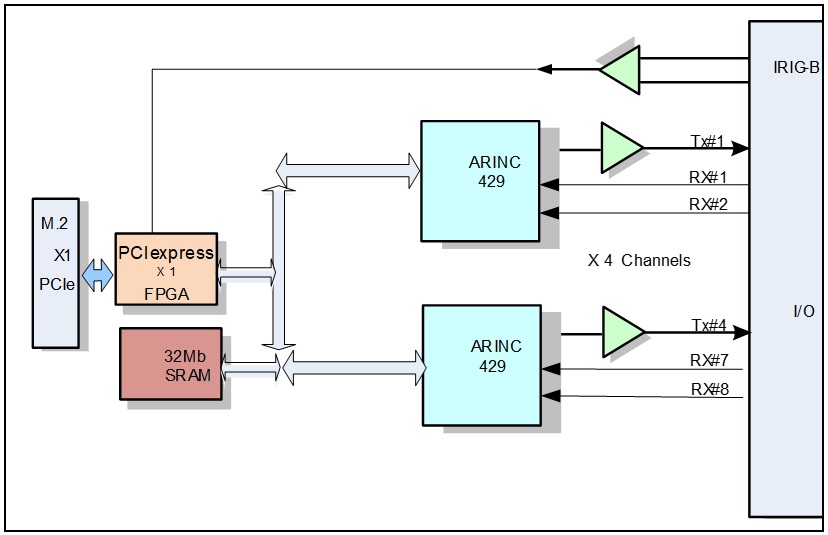
- ARINC 429-based M.2 card ARINC controller
- M.2 PCI Express x1 lane interface
- M.2 2260 support Key B & M
- Up to 4 transmitter and 8 receiver channels for ARINC controller
- Programmable label recognition for 256 labels per channel
- 32 x 32 Receive FIFOs and priority-label buffers
- Dependent data rates for transmit and receive
- Meets the ARINC 429 specifications for loading, level detection, timing, and protocol
M.2-ARINC429
M.2 22X60 B & M Key PCIe x1 ARINC 429 Controller up to 4 TX and 8 RX
- ARINC 429-based M.2 card ARINC controller
- M.2 PCI Express x1 lane interface
- M.2 2260 support Key B & M
- Up to 4 transmitter and 8 receiver channels for ARINC controller
- Programmable label recognition for 256 labels per channel
- 32 x 32 Receive FIFOs and priority-label buffers
- Dependent data rates for transmit and receive
- Meets the ARINC 429 specifications for loading, level detection, timing, and protocol
Share this product
LinkedIn
M.2-ARINC429
M.2 22X60 B & M Key PCIe x1 ARINC 429 Controller up to 4 TX and 8 RX
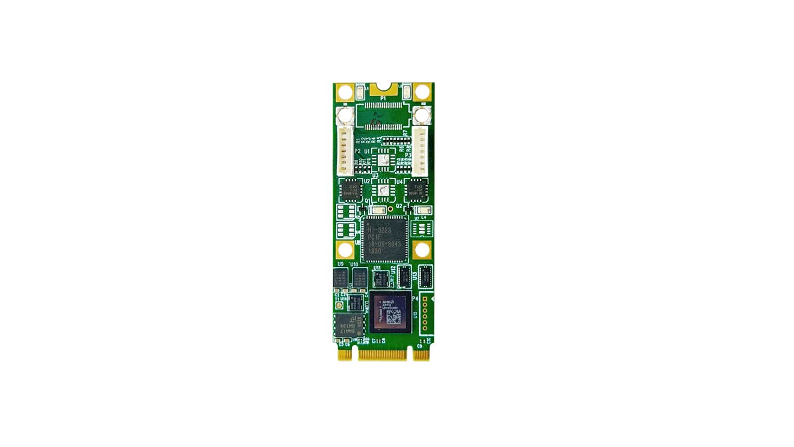
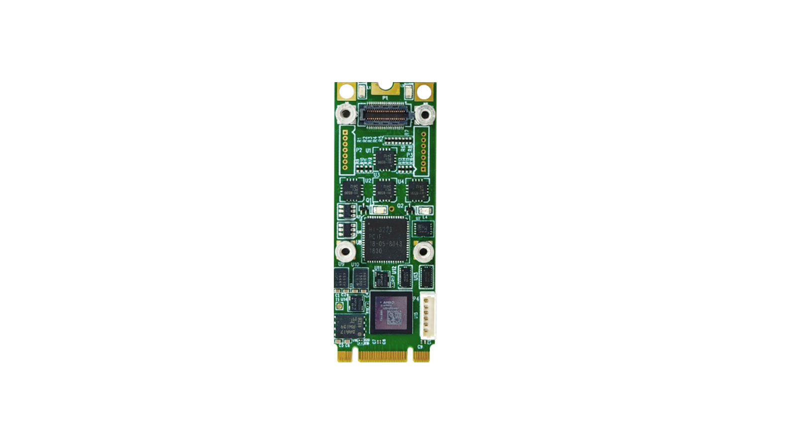
The M.2-ARINC429-4/8 (M.2 22mm x 60mm) board has an ARINC controller that supports ARINC 429 specifications. ARINC 429 (Aeronautical Radio Incorporated) is a specification that defines how avionics equipment and systems should communicate with each other. ARINC 429 employs a unidirectional data bus standard known as Mark 33 Digital Information Transfer System (DITS). Messages are transmitted and received at a bit rate of either 12.5kb/s or 100kb/s. The receiver input circuitry and logic are designed to directly meet the ARINC 429 specifications. The transmitter section provides the ARINC 429 communication protocol. The SPI data bus on the ARINC controller exchanges the 32-bit ARINC data word in two steps when either loading the transmitter or interrogating the receivers. The SRAM stores received data and transmitted data.
Full Technical Specs
- ARINC 429-based M.2 card ARINC controller
- M.2 PCI Express x1 lane interface
- M.2 2260 support Key B & M
- Up to 4 transmitter and 8 receiver channels for ARINC controller
- Programmable label recognition for 256 labels per channel
- 32 x 32 Receive FIFOs and priority-label buffers
- Dependent data rates for transmit and receive
- Meets the ARINC 429 specifications for loading, level detection, timing, and protocol
- Software selected data rate of 12.5kb/s or 100kb/s with automatic slew rate adjustment
- Burst and continuous mode available
- Programmable word length selection, with the parity bit generated automatically
- Programmable interrupt support
- Differential IRIG B input
Please: Contact Us
Data Sheet – Link Here
- ARINC 429-based M.2 card ARINC controller
- M.2 PCI Express x1 lane interface
- M.2 2260 support Key B & M
- Up to 4 transmitter and 8 receiver channels for ARINC controller
- Programmable label recognition for 256 labels per channel
- 32 x 32 Receive FIFOs and priority-label buffers
- Dependent data rates for transmit and receive
- Meets the ARINC 429 specifications for loading, level detection, timing, and protocol
| Mechanical Interface | Switched Mezzanine Card (XMC) Interface confirming to ANSI/VITA 42.0-2008 (Auxiliary Standard) Standard single-width (149mm x 74mm) | |||||||||
| Electrical Interface | PCI Express x4 Link (Base Specification 2.1) compliant interface conforming to ANSI/VITA 42.3-2006 (PCI Express Protocol Layer Standard) | |||||||||
| PCI Express Switch | PI7C9X2G312GP (Pericom) | |||||||||
| PCI Express to PCI Bridge | XIO2001 (Texas Instruments) | |||||||||
| User configurable FPGA | TXMC639-10R: XC7K160T-2FBG676I (AMD) TXMC639-11R: XC7K325T-2FBG676I (AMD) | |||||||||
| SPI-Flash | MT25QL128 (Micron) 128 Mbit (contains TXMC639 FPGA BRD) or compatible; +3.3 V supply voltage | |||||||||
| DDR3 RAM | 2x MT41K256M16TW-107 (Micron) 256Meg x 32 bit | |||||||||
| Board Configuration Controller | LCMXO2-7000HC (Lattice) | |||||||||
| ADC | LTC2320 -16 (Analog Devices) | |||||||||
| DAC | AD5547BRUZ (Analog Devices) | |||||||||
| A/D Channels | TXMC639-10R: 8 Differential 16bit A/D Channels TXMC639-11R: 16 Differential 16bit A/D Channels Input Configuration per BCC Device: Input Voltage Ranges: Differental : ±20.57 V, ±10.28 V or ±5.14 V (Single-Ended: ±10.28 V, ±5.14 V or ±2.57 V) All analog inputs are connected via an impedance converter and a second operation amplifier for level adjustment and filtering to the differential ADC inputs. The -3 dB limit of this input stage is at approx. 8MHz | |||||||||
| D/A Channels | TXMC639-10R: 4 Single-Ended 16 Bit D/A Channels TXMC639-11R: 8 Single-Ended 16 Bit D/A Channels Output range configurable per D/A channel. Maximum single-ended Output Voltage – Vout: ±10 V Maximum Output Drive Current for each Output: 10 mA Maximum Capacitive Load for each Output: 1000 pF Typical Settling Time for a 10 mA / 1000 pF: < 1 µs | |||||||||
| Digital Front I/O Channels | 32 digital I/O Lines
| |||||||||
| Digital Rear I/O Channels | 64 direct FPGA I/O lines to P14 Rear I/O connector
4 MGT line to P16 Rear I/O connector
| |||||||||
| Front I/O | Front I/O Samtec – ERF8_050_01_L_D_RA_L_TR | |||||||||
| P14 Rear I/O | 64 pin Mezzanine Connector (Molex 71436-2864 or compatible) | |||||||||
| P16 Rear I/O | 114 pin Mezzanine Connector (Samtec – ASP-105885-01) | |||||||||
| Power Requirements 1) | Depends on FPGA design With TXMC639 Board Reference Design / without external load
| |||||||||
| Temperature Range | Operating: – 40 °C to + 85 °C Storage: – 55 °C to + 125 °C | |||||||||
| MTBF 1) | 157 000 h to 161 000 h | |||||||||
| Humidity | 5% – 95% non-condensing | |||||||||
| Weight | 140 g |
1) depends on variant, for further details see User Manual
TXMC639-10R
| 8x Analog In, 4x Analog Out, XC7K160T-2FBG676 Kintex™ 7 FPGA AMD Kintex™ 7 FPGA (XC7K160T-2FBG676), 1GB DDR3, 8x Analog In, 4x Analog Out, 32x digital Front I/O, 64x direct FPGA Rear I/O Lines and 4x MGTs Rear I/O |
TXMC639-11R
| 16x Analog In, 8x Analog Out, XC7K325T-2FBG676 Kintex™ 7 FPGA AMD Kintex™ 7 FPGA (XC7K325T-2FBG676), 1GB DDR3, 16x Analog In, 8x Analog Out, 32x digital Front I/O, 64x direct FPGA Rear I/O Lines and 4x MGTs Rear I/O |
SOFTWARE
Share this product
LinkedIn


