- Form Factor: M.2 30mm x 42mm, Key B & M
- Interface: M.2 PCI Express x1 lane
- Time Synchronization Inputs:
- IRIG A, B, NASA 36, 1 PPS sync inputs
- HaveQuick sync input
- Time Code Output: IRIG-B time code output
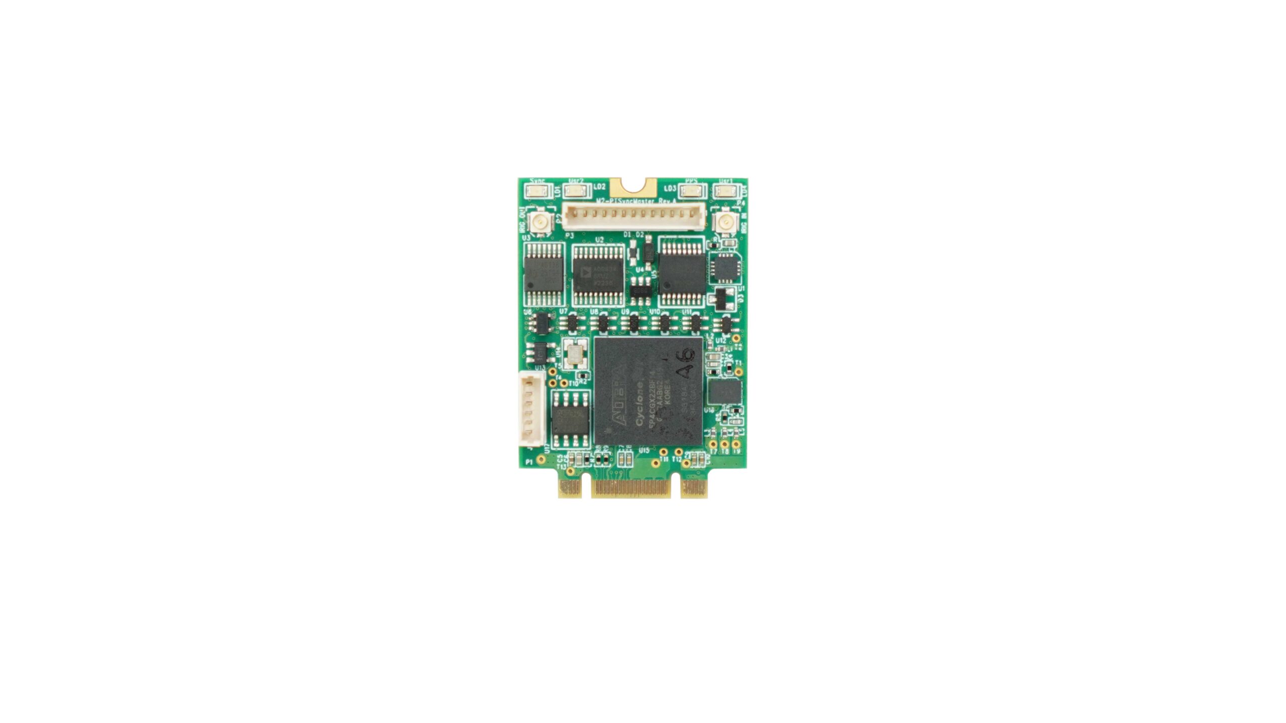

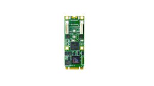
M.2-PTSyncMaster
Precision Time Master Reference M.2 30x42mm
- Form Factor: M.2 30mm x 42mm, Key B & M
- Interface: M.2 PCI Express x1 lane
- Time Synchronization Inputs:
- IRIG A, B, NASA 36, 1 PPS sync inputs
- HaveQuick sync input
- Time Code Output: IRIG-B time code output
Share this product
LinkedIn
M.2-PTSyncMaster
Precision Time Master Reference M.2 30x42mm
The M.2-PTSyncMaster module provides its host system with a zero-latency Precision Time Master reference. It accepts various reference signal inputs, including 1 PPS, IRIG, NASA, or HaveQuick. The clock supports IRIG A, B, or NASA 36 input formats and allows for user input of reference signal delay information. An IRIG B code generator is also included. Advanced features such as Event Time input, Match Time, and Heartbeat Timing offer the host system comprehensive Precision Time Master reference capabilities. These features enable precise synchronization and timing, making it suitable for applications requiring high accuracy and reliability. The M.2-PTSyncMaster module continuously measures the time error between its onboard clock and a reference input, adjusting for propagation delay. An adaptive gain loop uses the residual error to adjust the oscillator’s frequency, minimizing error. If the incoming time code is missing or corrupted, the onboard clock is updated using a TCXO until the input code becomes available. The module features an Event Time input to capture the exact time of external events with a resolution of 100 ns. The Match Time feature can initiate or terminate processes with a resolution of 1 μs, asserting a Match Ready status when the clock’s time matches the user-input start time. The output is terminated under user control or when a pre-programmed stop time occurs. Additionally, a programmable Heartbeat Timing generator is available over a range of 2 to 65,535, with a selectable divider for 3 MHz or 100 Hz. Time data are provided via 58 bits of BCD, allowing for zero-latency time reads that include units from microseconds to years, along with an additional status byte.
All Features
- Form Factor: M.2 30mm x 42mm, Key B & M
- Interface: M.2 PCI Express x1 lane
- Time Synchronization Inputs:
- IRIG A, B, NASA 36, 1 PPS sync inputs
- HaveQuick sync input
- Time Code Output: IRIG-B time code output
- Clock Features:
- Disciplined TCXO (Temperature Compensated Crystal Oscillator)
- Zero latency time reads
- Propagation delay correction
- Event Time Tagging: External event time tagging with 100ns resolution
- Match Time Feature: Initiates or terminates processes with 1μs resolution
- Heartbeat Timing: Programmable heartbeat rate interrupt
- GPS Interface: RS-232 interface for GPS connectivity
Input/Output Specifications
- Input codes: IRIG A, B, NASA 36 (1 kHz carrier)
- Input amplitude: 0.25 to 10 Vpp
- Input impedance: >10 kΩ
- Ratio: 2:1 to 6:1
- Frequency error: 100 PPM max
- Code sync accuracy: 1 μs
- 1PPS input: TTL, positive edge
- External event input: TTL, positive or negative edge
- Resolution: 100 ns to units of year
- Minimum event spacing: None
Time Data and Status
- BCD time: Microseconds to years, available on demand with zero latency
- Time data format: 58 bits in two 32-bit words
- Status word: 8 bits
- Status LED: Flashing coded patterns
Interrupts and Flags
- Interrupts:
- External event
- RAM FIFO
- Heartbeat
- Match time
- Flags:
- Dual-port RAM data ready
- FIFO data ready
- In sync
- Heartbeat
- Match time
- External event
Connectors
- U.FL micro coax
- 10-pin Picoblade GPS connector
Operating Environment
- Operating temperature:
- Industrial: -40°C to +85°C
- Non-operating temperature: -50°C to +90°C
- Airflow requirement: 0.5 CFM
- Humidity: 5 to 90% (non-condensing)
- Altitude: Up to 10,000 feet
Software Drivers
- Linux drivers
- Windows drivers
- VxWorks drivers
Mechanical Specifications
- Size: M.2 Key B & M (30mm x 42mm)
- Power consumption: 5W max
- Front panel I/O options
- Vibration resistance: 0.5G, 20-2000 Hz random
- Shock resistance: 20G, 11 ms, ½ sine
- Weight: Approximately 10g (0.4 oz)
- MTBF: >250,000 hours
Part Number: M.2-PTSyncMaster
-
- Precision Time Master Reference
- Option: Add “C” to the part number for Conformal Coat
Optional Accessories:
- Part Number: CBL-MINI-10-12
- 10 pins housing to 12“ pigtail
- Form Factor: M.2 30mm x 42mm, Key B & M
- Interface: M.2 PCI Express x1 lane
- Time Synchronization Inputs:
- IRIG A, B, NASA 36, 1 PPS sync inputs
- HaveQuick sync input
- Time Code Output: IRIG-B time code output
| Mechanical Interface | Switched Mezzanine Card (XMC) Interface confirming to ANSI/VITA 42.0-2008 (Auxiliary Standard) Standard single-width (149mm x 74mm) | |||||||||
| Electrical Interface | PCI Express x4 Link (Base Specification 2.1) compliant interface conforming to ANSI/VITA 42.3-2006 (PCI Express Protocol Layer Standard) | |||||||||
| PCI Express Switch | PI7C9X2G312GP (Pericom) | |||||||||
| PCI Express to PCI Bridge | XIO2001 (Texas Instruments) | |||||||||
| User configurable FPGA | TXMC639-10R: XC7K160T-2FBG676I (AMD) TXMC639-11R: XC7K325T-2FBG676I (AMD) | |||||||||
| SPI-Flash | MT25QL128 (Micron) 128 Mbit (contains TXMC639 FPGA BRD) or compatible; +3.3 V supply voltage | |||||||||
| DDR3 RAM | 2x MT41K256M16TW-107 (Micron) 256Meg x 32 bit | |||||||||
| Board Configuration Controller | LCMXO2-7000HC (Lattice) | |||||||||
| ADC | LTC2320 -16 (Analog Devices) | |||||||||
| DAC | AD5547BRUZ (Analog Devices) | |||||||||
| A/D Channels | TXMC639-10R: 8 Differential 16bit A/D Channels TXMC639-11R: 16 Differential 16bit A/D Channels Input Configuration per BCC Device: Input Voltage Ranges: Differental : ±20.57 V, ±10.28 V or ±5.14 V (Single-Ended: ±10.28 V, ±5.14 V or ±2.57 V) All analog inputs are connected via an impedance converter and a second operation amplifier for level adjustment and filtering to the differential ADC inputs. The -3 dB limit of this input stage is at approx. 8MHz | |||||||||
| D/A Channels | TXMC639-10R: 4 Single-Ended 16 Bit D/A Channels TXMC639-11R: 8 Single-Ended 16 Bit D/A Channels Output range configurable per D/A channel. Maximum single-ended Output Voltage – Vout: ±10 V Maximum Output Drive Current for each Output: 10 mA Maximum Capacitive Load for each Output: 1000 pF Typical Settling Time for a 10 mA / 1000 pF: < 1 µs | |||||||||
| Digital Front I/O Channels | 32 digital I/O Lines
| |||||||||
| Digital Rear I/O Channels | 64 direct FPGA I/O lines to P14 Rear I/O connector
4 MGT line to P16 Rear I/O connector
| |||||||||
| Front I/O | Front I/O Samtec – ERF8_050_01_L_D_RA_L_TR | |||||||||
| P14 Rear I/O | 64 pin Mezzanine Connector (Molex 71436-2864 or compatible) | |||||||||
| P16 Rear I/O | 114 pin Mezzanine Connector (Samtec – ASP-105885-01) | |||||||||
| Power Requirements 1) | Depends on FPGA design With TXMC639 Board Reference Design / without external load
| |||||||||
| Temperature Range | Operating: – 40 °C to + 85 °C Storage: – 55 °C to + 125 °C | |||||||||
| MTBF 1) | 157 000 h to 161 000 h | |||||||||
| Humidity | 5% – 95% non-condensing | |||||||||
| Weight | 140 g |
1) depends on variant, for further details see User Manual
TXMC639-10R
| 8x Analog In, 4x Analog Out, XC7K160T-2FBG676 Kintex™ 7 FPGA AMD Kintex™ 7 FPGA (XC7K160T-2FBG676), 1GB DDR3, 8x Analog In, 4x Analog Out, 32x digital Front I/O, 64x direct FPGA Rear I/O Lines and 4x MGTs Rear I/O |
TXMC639-11R
| 16x Analog In, 8x Analog Out, XC7K325T-2FBG676 Kintex™ 7 FPGA AMD Kintex™ 7 FPGA (XC7K325T-2FBG676), 1GB DDR3, 16x Analog In, 8x Analog Out, 32x digital Front I/O, 64x direct FPGA Rear I/O Lines and 4x MGTs Rear I/O |
SOFTWARE
Share this product
LinkedIn