- Drop-in replacement for SBS IP-ADIO
- Up to 16 single-ended or 8 differential analog inputs
- 13-bit ADC (from 1X to 128X) yielding a 21-bit effective dynamic input range
- ±10V maximum input with ±44V overvoltage protection
- 24-bit pacer clock for ADC and DAC
- 17µs analog sample rate (50kHz maximum throughput)
- Hardware autozero and autocalibration, factory trim
- 16-bit interface
- 2 deglitched analog outputs with 3 independent output ranges
- DACs double buffered with pacer clock
- Up to 68 digital I/O lines
- Up to 12 interrupt sources
- 2 24-bit general purpose timers
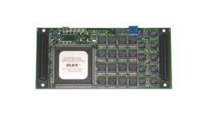
IP-ADIO
Double-size Programmable Analog and Digital I/O
- Drop-in replacement for SBS IP-ADIO
- Up to 16 single-ended or 8 differential analog inputs
- 13-bit ADC (from 1X to 128X) yielding a 21-bit effective dynamic input range
- ±10V maximum input with ±44V overvoltage protection
- 24-bit pacer clock for ADC and DAC
- 17µs analog sample rate (50kHz maximum throughput)
- Hardware autozero and autocalibration, factory trim
- 16-bit interface
- 2 deglitched analog outputs with 3 independent output ranges
- DACs double buffered with pacer clock
- Up to 68 digital I/O lines
- Up to 12 interrupt sources
- 2 24-bit general purpose timers
Share this product
LinkedIn
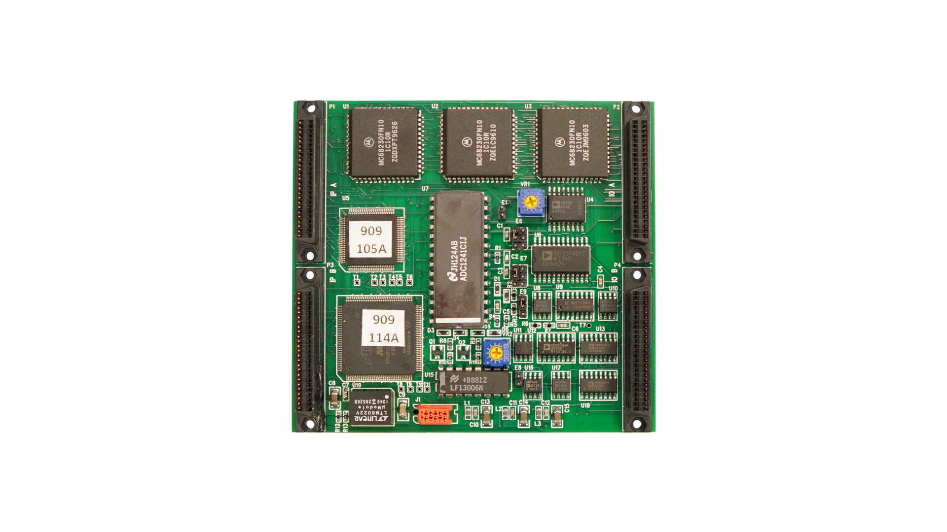
IP-ADIO
Double-size Programmable Analog and Digital I/O
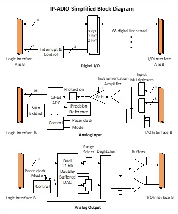
Analog Inputs
The IP-ADIO has 16 analog inputs. Each input passes through an 8-step programmable gain amplifier before being routed to a 13-bit ADC. The analog input range is ±10V full scale, with ±44V overvoltage protection. The amplifier gives a gain of 1X to 128X in eight steps of 2ⁿ=0..7, which yields a 21-bit effective dynamic input range. Typical acquisition-conversion time is 17µs, which gives a maximum nominal throughput of 50kHz. A software selectable high-speed mode doubles throughput, with reduced analog specifications.
Analog Outputs
The IP-ADIO has two 12-bit deglitched analog output channels, with three available independent output ranges: 0 to +5V; 0 to +10V; and ±5V. The output interval is programmable from 4µs to over 60s in 4µs intervals. The DACs are double-buffered, which eliminates timing-induced output jitter.
Digital Inputs/Outputs
Up to 68 digital I/O lines are available. Each connects to one of three MC68230 Programmable Interface/Timers.
Applications:
- Process control
- Industrial control
- Precision instrumentation
- Data acquisition systems (DAS)
Available Software Drivers:
- C library dll’s
- Linux drivers
- Windows drivers
- VxWorks drivers
Mechanical:
- Double-size Industry Pack
- 1.800in x 3.900in (45.72mm x 99.06mm)
- Front panel I/O
- Vibration: 0.5G, 20-2000Hz rand
- Shock: 20G, 11msec, 1⁄2 sine
- MTBF: >250,000 hours
Operating Environment:
- Operating temperature: Industrial -40oC to +85oC
- Humidity: 5 to 90% (non-cond)
- Altitude: 0 to 10,000 feet
IP-ADIO:
Double-size Industry Pack, 16 Analog Inputs, 2 Analog Outputs, 68 Digital I/O
Temp: -40oC to +85oC
- Drop-in replacement for SBS IP-ADIO
- Up to 16 single-ended or 8 differential analog inputs
- 13-bit ADC (from 1X to 128X) yielding a 21-bit effective dynamic input range
- ±10V maximum input with ±44V overvoltage protection
- 24-bit pacer clock for ADC and DAC
- 17µs analog sample rate (50kHz maximum throughput)
- Hardware autozero and autocalibration, factory trim
- 16-bit interface
- 2 deglitched analog outputs with 3 independent output ranges
- DACs double buffered with pacer clock
- Up to 68 digital I/O lines
- Up to 12 interrupt sources
- 2 24-bit general purpose timers
| Mechanical Interface | Switched Mezzanine Card (XMC) Interface confirming to ANSI/VITA 42.0-2008 (Auxiliary Standard) Standard single-width (149mm x 74mm) | |||||||||
| Electrical Interface | PCI Express x4 Link (Base Specification 2.1) compliant interface conforming to ANSI/VITA 42.3-2006 (PCI Express Protocol Layer Standard) | |||||||||
| PCI Express Switch | PI7C9X2G312GP (Pericom) | |||||||||
| PCI Express to PCI Bridge | XIO2001 (Texas Instruments) | |||||||||
| User configurable FPGA | TXMC639-10R: XC7K160T-2FBG676I (AMD) TXMC639-11R: XC7K325T-2FBG676I (AMD) | |||||||||
| SPI-Flash | MT25QL128 (Micron) 128 Mbit (contains TXMC639 FPGA BRD) or compatible; +3.3 V supply voltage | |||||||||
| DDR3 RAM | 2x MT41K256M16TW-107 (Micron) 256Meg x 32 bit | |||||||||
| Board Configuration Controller | LCMXO2-7000HC (Lattice) | |||||||||
| ADC | LTC2320 -16 (Analog Devices) | |||||||||
| DAC | AD5547BRUZ (Analog Devices) | |||||||||
| A/D Channels | TXMC639-10R: 8 Differential 16bit A/D Channels TXMC639-11R: 16 Differential 16bit A/D Channels Input Configuration per BCC Device: Input Voltage Ranges: Differental : ±20.57 V, ±10.28 V or ±5.14 V (Single-Ended: ±10.28 V, ±5.14 V or ±2.57 V) All analog inputs are connected via an impedance converter and a second operation amplifier for level adjustment and filtering to the differential ADC inputs. The -3 dB limit of this input stage is at approx. 8MHz | |||||||||
| D/A Channels | TXMC639-10R: 4 Single-Ended 16 Bit D/A Channels TXMC639-11R: 8 Single-Ended 16 Bit D/A Channels Output range configurable per D/A channel. Maximum single-ended Output Voltage – Vout: ±10 V Maximum Output Drive Current for each Output: 10 mA Maximum Capacitive Load for each Output: 1000 pF Typical Settling Time for a 10 mA / 1000 pF: < 1 µs | |||||||||
| Digital Front I/O Channels | 32 digital I/O Lines
| |||||||||
| Digital Rear I/O Channels | 64 direct FPGA I/O lines to P14 Rear I/O connector
4 MGT line to P16 Rear I/O connector
| |||||||||
| Front I/O | Front I/O Samtec – ERF8_050_01_L_D_RA_L_TR | |||||||||
| P14 Rear I/O | 64 pin Mezzanine Connector (Molex 71436-2864 or compatible) | |||||||||
| P16 Rear I/O | 114 pin Mezzanine Connector (Samtec – ASP-105885-01) | |||||||||
| Power Requirements 1) | Depends on FPGA design With TXMC639 Board Reference Design / without external load
| |||||||||
| Temperature Range | Operating: – 40 °C to + 85 °C Storage: – 55 °C to + 125 °C | |||||||||
| MTBF 1) | 157 000 h to 161 000 h | |||||||||
| Humidity | 5% – 95% non-condensing | |||||||||
| Weight | 140 g |
1) depends on variant, for further details see User Manual
TXMC639-10R
| 8x Analog In, 4x Analog Out, XC7K160T-2FBG676 Kintex™ 7 FPGA AMD Kintex™ 7 FPGA (XC7K160T-2FBG676), 1GB DDR3, 8x Analog In, 4x Analog Out, 32x digital Front I/O, 64x direct FPGA Rear I/O Lines and 4x MGTs Rear I/O |
TXMC639-11R
| 16x Analog In, 8x Analog Out, XC7K325T-2FBG676 Kintex™ 7 FPGA AMD Kintex™ 7 FPGA (XC7K325T-2FBG676), 1GB DDR3, 16x Analog In, 8x Analog Out, 32x digital Front I/O, 64x direct FPGA Rear I/O Lines and 4x MGTs Rear I/O |
SOFTWARE
Share this product
LinkedIn