- 8 Channels 16-bit A/D converter, Simultaneously Sampled
- Fast throughput rate: 200 KSPS for all 8 channels
- 8 Channels SE or 4 PSEUDO Differentials
- Single-ended or 4 differential channels
- True bipolar analog input ranges: ±10 V, ±5 V, selection applies to all Channels
- Analog Input Clamp Protection
- 1MΩ Analog Input Impedance
- Programmable 2nd Order Anti-alias Analog Filter
- Over-sampling capability with digital filter
- 8Kx16 SRAM
- PCIexpress compliant

PCIe-Mini-AD8200
Mini 8 Channels 16-bit, 200KSPS For All 8 Channels
- 8 Channels 16-bit A/D converter, Simultaneously Sampled
- Fast throughput rate: 200 KSPS for all 8 channels
- 8 Channels SE or 4 PSEUDO Differentials
- Single-ended or 4 differential channels
- True bipolar analog input ranges: ±10 V, ±5 V, selection applies to all Channels
- Analog Input Clamp Protection
- 1MΩ Analog Input Impedance
- Programmable 2nd Order Anti-alias Analog Filter
- Over-sampling capability with digital filter
- 8Kx16 SRAM
- PCIexpress compliant
Share this product
LinkedIn
PCIe-Mini-AD8200
Mini 8 Channels 16-bit, 200KSPS For All 8 Channels
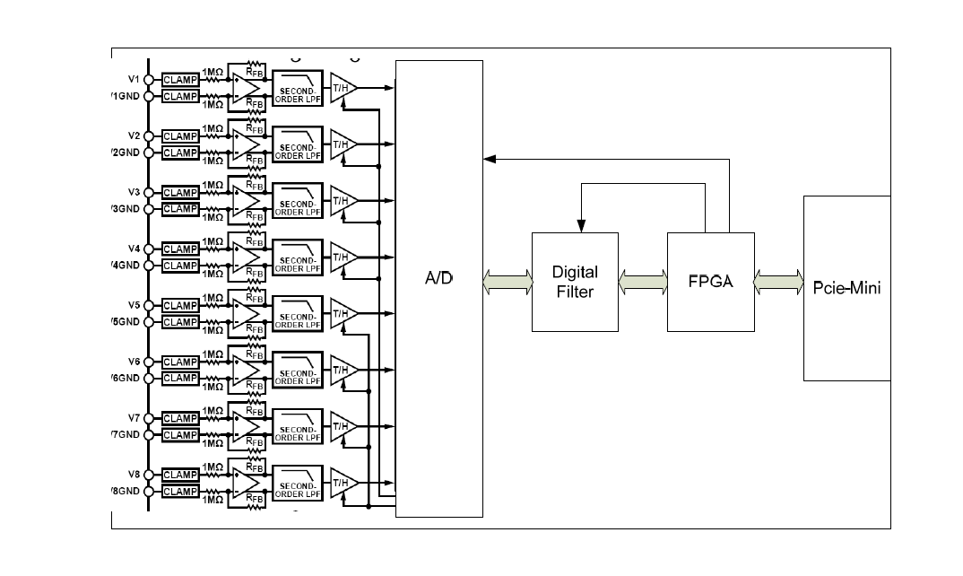
The PCIe-Mini-AD8200 Simultaneously Sampled A/D offers a mix of up to 8 single-ended or 4 differential analog input channels. All channel features programmable gain 1 or 2 and can program to handle analog input with a single-ended or differential configuration. The acquisition can be started by the host or by an on-board sequencer that uses a channel list to specify which channel to acquire. A local 8Kx16 but dual ported SRAM stores the acquisition data. Memory pointers can be selected t limit the number of scans gathered, as well as the control of interrupt generation. The 16-bit A/D converters can provide a global acquisition and conversion time of ≤5μsec per sample per channel.
The board offers a programmable digital filter:
±5 V range, the −3 dB frequency is typically 15 kHz. In the ±10 V range, the −3 dB frequency is typically 23 kHz.
Applications:
- Process control
- Industrial control
- Precision instrumentation
- Data acquisition systems (DAS)
- Multiaxis positioning systems
A/D Device Specifications:
- 16-bit, charge redistribution SAR, A/D converter
- Hardware factory-calibrated and tested to ensure SNR and THD are within specifications
- Gain, offset, and linearity are also factory calibrated
- Throughput: 200 KSPS
- INL: ±0.5 LSB Max with no missing code
- 95.5 dB SNR, −107 dB THD
- Analog input voltage ranges: Bipolar ±10 V, ±5 V
- 7 kV ESD rating on analog input channels
- No pipeline delay
Mechanical / Environmental:
- Size: Mini PCI Type III Module, 44.6mm x 59.8mm
- Power: T.B.D.
- Front panel I/O
- Vibration: 0.5G, 20-2000 Hz rand
- Shock: 20G, 11 msec, ½ sine
- Weight: T.B.D.
- MTBF: >250,000 hours
Operating Environment:
- Operating temperature: -40 ºC to +85 ºC
- Airflow requirement: 5 CFM
- Humidity: 5 to 90% (non-condensing)
- Altitude: 0 to 10,000 feet
Ordering Information:
- Part number: PCIe-Mini-AD8200
- 8 Channels 16 Bits, 200KSP
- Ext Temp: -40 ºC to +85 ºC
Data Sheet – Link Here
- 8 Channels 16-bit A/D converter, Simultaneously Sampled
- Fast throughput rate: 200 KSPS for all 8 channels
- 8 Channels SE or 4 PSEUDO Differentials
- Single-ended or 4 differential channels
- True bipolar analog input ranges: ±10 V, ±5 V, selection applies to all Channels
- Analog Input Clamp Protection
- 1MΩ Analog Input Impedance
- Programmable 2nd Order Anti-alias Analog Filter
- Over-sampling capability with digital filter
- 8Kx16 SRAM
- PCIexpress compliant
| Mechanical Interface | Switched Mezzanine Card (XMC) Interface confirming to ANSI/VITA 42.0-2008 (Auxiliary Standard) Standard single-width (149mm x 74mm) | |||||||||
| Electrical Interface | PCI Express x4 Link (Base Specification 2.1) compliant interface conforming to ANSI/VITA 42.3-2006 (PCI Express Protocol Layer Standard) | |||||||||
| PCI Express Switch | PI7C9X2G312GP (Pericom) | |||||||||
| PCI Express to PCI Bridge | XIO2001 (Texas Instruments) | |||||||||
| User configurable FPGA | TXMC639-10R: XC7K160T-2FBG676I (AMD) TXMC639-11R: XC7K325T-2FBG676I (AMD) | |||||||||
| SPI-Flash | MT25QL128 (Micron) 128 Mbit (contains TXMC639 FPGA BRD) or compatible; +3.3 V supply voltage | |||||||||
| DDR3 RAM | 2x MT41K256M16TW-107 (Micron) 256Meg x 32 bit | |||||||||
| Board Configuration Controller | LCMXO2-7000HC (Lattice) | |||||||||
| ADC | LTC2320 -16 (Analog Devices) | |||||||||
| DAC | AD5547BRUZ (Analog Devices) | |||||||||
| A/D Channels | TXMC639-10R: 8 Differential 16bit A/D Channels TXMC639-11R: 16 Differential 16bit A/D Channels Input Configuration per BCC Device: Input Voltage Ranges: Differental : ±20.57 V, ±10.28 V or ±5.14 V (Single-Ended: ±10.28 V, ±5.14 V or ±2.57 V) All analog inputs are connected via an impedance converter and a second operation amplifier for level adjustment and filtering to the differential ADC inputs. The -3 dB limit of this input stage is at approx. 8MHz | |||||||||
| D/A Channels | TXMC639-10R: 4 Single-Ended 16 Bit D/A Channels TXMC639-11R: 8 Single-Ended 16 Bit D/A Channels Output range configurable per D/A channel. Maximum single-ended Output Voltage – Vout: ±10 V Maximum Output Drive Current for each Output: 10 mA Maximum Capacitive Load for each Output: 1000 pF Typical Settling Time for a 10 mA / 1000 pF: < 1 µs | |||||||||
| Digital Front I/O Channels | 32 digital I/O Lines
| |||||||||
| Digital Rear I/O Channels | 64 direct FPGA I/O lines to P14 Rear I/O connector
4 MGT line to P16 Rear I/O connector
| |||||||||
| Front I/O | Front I/O Samtec – ERF8_050_01_L_D_RA_L_TR | |||||||||
| P14 Rear I/O | 64 pin Mezzanine Connector (Molex 71436-2864 or compatible) | |||||||||
| P16 Rear I/O | 114 pin Mezzanine Connector (Samtec – ASP-105885-01) | |||||||||
| Power Requirements 1) | Depends on FPGA design With TXMC639 Board Reference Design / without external load
| |||||||||
| Temperature Range | Operating: – 40 °C to + 85 °C Storage: – 55 °C to + 125 °C | |||||||||
| MTBF 1) | 157 000 h to 161 000 h | |||||||||
| Humidity | 5% – 95% non-condensing | |||||||||
| Weight | 140 g |
1) depends on variant, for further details see User Manual
TXMC639-10R
| 8x Analog In, 4x Analog Out, XC7K160T-2FBG676 Kintex™ 7 FPGA AMD Kintex™ 7 FPGA (XC7K160T-2FBG676), 1GB DDR3, 8x Analog In, 4x Analog Out, 32x digital Front I/O, 64x direct FPGA Rear I/O Lines and 4x MGTs Rear I/O |
TXMC639-11R
| 16x Analog In, 8x Analog Out, XC7K325T-2FBG676 Kintex™ 7 FPGA AMD Kintex™ 7 FPGA (XC7K325T-2FBG676), 1GB DDR3, 16x Analog In, 8x Analog Out, 32x digital Front I/O, 64x direct FPGA Rear I/O Lines and 4x MGTs Rear I/O |
SOFTWARE
Share this product
LinkedIn


