- MIL-STD-1553 Compliance: Compliant with MIL-STD-1553B
- Modes: Supports Bus Controller (BC), Remote Terminal (RT), and Bus Monitor (BM) modes
- Dual Redundancy: Dual redundant 1553B BC/RT/BM modes
- Connectors: Dual tri-axial front panel connectors
- Message Processing: Multiple message processing in BC and RT modes


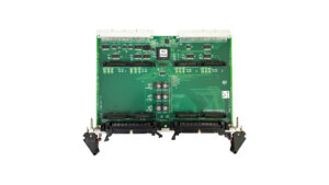
VME-MIL-STD-1553B
VME-MIL-STD-1553B Dual Redundant Controller Bus Controller / Remote Terminal / Bus Monitor
- MIL-STD-1553 Compliance: Compliant with MIL-STD-1553B
- Modes: Supports Bus Controller (BC), Remote Terminal (RT), and Bus Monitor (BM) modes
- Dual Redundancy: Dual redundant 1553B BC/RT/BM modes
- Connectors: Dual tri-axial front panel connectors
- Message Processing: Multiple message processing in BC and RT modes
Share this product
LinkedIn
VME-MIL-STD-1553B
VME-MIL-STD-1553B Dual Redundant Controller Bus Controller / Remote Terminal / Bus Monitor
The VME-1553-x BCRTM Module is a high-performance, 6U module based on the BCRTM 1553 chip, supporting MIL-STD-1553B standards. It offers options for operating temperatures ranging from 0 to +70 degrees Celsius and -40 to +85 degrees Celsius, with the option for conformal coating. The module supports up to four channels of dual-redundant 1553 bus per channel. It includes 128 Kbyte SRAM and operates in BC (Bus Controller), RT (Remote Terminal), and M (Monitor) modes. The module features dual redundant channels (A and B), 78 ohm transformers, and supports both long and short stub configurations. It includes internal and external clock options and separate logic for the VME interface, ensuring low power consumption. LED status indicators are provided, and software libraries are available for ‘C’, Windows, Linux, and VxWorks, with PICMG compliance.
Module Features
- UTMC BCRTM controller
- 128Kbytes SRAM
- On-chip transceivers
- On-board transformers
- Long and short stub configurations supported
Memory
- 128 Kbyte external SRAM
I/O Capabilities
- Up to four 1553 bus levels
- TTL (5v) clock
Programmability
- Programmable via VME Bus
VME Interface
- A32/A24/A16 address modes with D16/D08 data modes
- Read, modify, and write cycles supported
- Interrupts: software-programmable from 1 to 7
Operating Environment
- Operating temperature: Commercial 0 to +55 °C, Optional -40°C to +85°C
- Airflow requirement: 0.5 CFM
- Humidity: 5 to 90% (non-cond.)
- Altitude: up to 10,000 ft
Mechanical Environment
- Size: 6U, 233 x 160mm
- Power consumption: 1.5 watts
- Front panel I/O
- Vibration resistance: 0.5G RMS (20-2000 Hz)
- Shock resistance: 20 G (11 ms, ½ sine)
- Weight: To be determined
- MTBF: >250,000 hours
Part Number: COM-1553B-X-Y
-
- X = 3 for 3U VME
- Y = C for Commercial (0° C to +70° C), I for Industrial (-40° C to +85° C), M for Military (MIL-STD-810D)
- MIL-STD-1553 Compliance: Compliant with MIL-STD-1553B
- Modes: Supports Bus Controller (BC), Remote Terminal (RT), and Bus Monitor (BM) modes
- Dual Redundancy: Dual redundant 1553B BC/RT/BM modes
- Connectors: Dual tri-axial front panel connectors
- Message Processing: Multiple message processing in BC and RT modes
| Mechanical Interface | Switched Mezzanine Card (XMC) Interface confirming to ANSI/VITA 42.0-2008 (Auxiliary Standard) Standard single-width (149mm x 74mm) | |||||||||
| Electrical Interface | PCI Express x4 Link (Base Specification 2.1) compliant interface conforming to ANSI/VITA 42.3-2006 (PCI Express Protocol Layer Standard) | |||||||||
| PCI Express Switch | PI7C9X2G312GP (Pericom) | |||||||||
| PCI Express to PCI Bridge | XIO2001 (Texas Instruments) | |||||||||
| User configurable FPGA | TXMC639-10R: XC7K160T-2FBG676I (AMD) TXMC639-11R: XC7K325T-2FBG676I (AMD) | |||||||||
| SPI-Flash | MT25QL128 (Micron) 128 Mbit (contains TXMC639 FPGA BRD) or compatible; +3.3 V supply voltage | |||||||||
| DDR3 RAM | 2x MT41K256M16TW-107 (Micron) 256Meg x 32 bit | |||||||||
| Board Configuration Controller | LCMXO2-7000HC (Lattice) | |||||||||
| ADC | LTC2320 -16 (Analog Devices) | |||||||||
| DAC | AD5547BRUZ (Analog Devices) | |||||||||
| A/D Channels | TXMC639-10R: 8 Differential 16bit A/D Channels TXMC639-11R: 16 Differential 16bit A/D Channels Input Configuration per BCC Device: Input Voltage Ranges: Differental : ±20.57 V, ±10.28 V or ±5.14 V (Single-Ended: ±10.28 V, ±5.14 V or ±2.57 V) All analog inputs are connected via an impedance converter and a second operation amplifier for level adjustment and filtering to the differential ADC inputs. The -3 dB limit of this input stage is at approx. 8MHz | |||||||||
| D/A Channels | TXMC639-10R: 4 Single-Ended 16 Bit D/A Channels TXMC639-11R: 8 Single-Ended 16 Bit D/A Channels Output range configurable per D/A channel. Maximum single-ended Output Voltage – Vout: ±10 V Maximum Output Drive Current for each Output: 10 mA Maximum Capacitive Load for each Output: 1000 pF Typical Settling Time for a 10 mA / 1000 pF: < 1 µs | |||||||||
| Digital Front I/O Channels | 32 digital I/O Lines
| |||||||||
| Digital Rear I/O Channels | 64 direct FPGA I/O lines to P14 Rear I/O connector
4 MGT line to P16 Rear I/O connector
| |||||||||
| Front I/O | Front I/O Samtec – ERF8_050_01_L_D_RA_L_TR | |||||||||
| P14 Rear I/O | 64 pin Mezzanine Connector (Molex 71436-2864 or compatible) | |||||||||
| P16 Rear I/O | 114 pin Mezzanine Connector (Samtec – ASP-105885-01) | |||||||||
| Power Requirements 1) | Depends on FPGA design With TXMC639 Board Reference Design / without external load
| |||||||||
| Temperature Range | Operating: – 40 °C to + 85 °C Storage: – 55 °C to + 125 °C | |||||||||
| MTBF 1) | 157 000 h to 161 000 h | |||||||||
| Humidity | 5% – 95% non-condensing | |||||||||
| Weight | 140 g |
1) depends on variant, for further details see User Manual
TXMC639-10R
| 8x Analog In, 4x Analog Out, XC7K160T-2FBG676 Kintex™ 7 FPGA AMD Kintex™ 7 FPGA (XC7K160T-2FBG676), 1GB DDR3, 8x Analog In, 4x Analog Out, 32x digital Front I/O, 64x direct FPGA Rear I/O Lines and 4x MGTs Rear I/O |
TXMC639-11R
| 16x Analog In, 8x Analog Out, XC7K325T-2FBG676 Kintex™ 7 FPGA AMD Kintex™ 7 FPGA (XC7K325T-2FBG676), 1GB DDR3, 16x Analog In, 8x Analog Out, 32x digital Front I/O, 64x direct FPGA Rear I/O Lines and 4x MGTs Rear I/O |
SOFTWARE
Share this product
LinkedIn