- User Programmable Altera Cyclone II FPGA 672 BGA:
- EP2C35
- EP2C50
- EP2C70
- Stand alone possibility
- Single wide PMC Module
- 64 LVTTL
- Optional User clock oscillator

PMC-CycloneII-64LVTTL
USER RECONFIGURABLE ALTERA FPGA,4MBYTE DUAL-PORTED SRAM,64LV TTL
- User Programmable Altera Cyclone II FPGA 672 BGA:
- EP2C35
- EP2C50
- EP2C70
- Stand alone possibility
- Single wide PMC Module
- 64 LVTTL
- Optional User clock oscillator
Share this product
LinkedIn
PMC-CycloneII-64LVTTL
USER RECONFIGURABLE ALTERA FPGA,4MBYTE DUAL-PORTED SRAM,64LV TTL
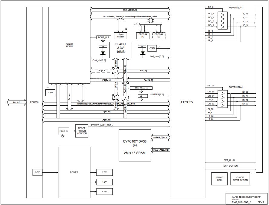
The Cyclone II EP2C35 FPGA in a 672-fbga package offers extensive customization options, featuring 4 Mbyte dual-ported SRAM, separate IP interface logic, reconfigurable I/O with 64 LVTTL lines, independent interrupt support for each GPIO line, user-configurable I/O by groups of 4 (2 pairs), on-board serial configuration device, local serial EPROM, internal/external clock options, PCI +3.3V/+5V operation, 32/64 MHz PMC clock support, front panel I/O access, and Windows and Linux drivers
Memory
- 4 Mbyte external SRAM
- Dual ported between the Altera and PMC bus with arbitration
I/O Level
- 64 I/O pins externally buffered LVTTL
- Fully User programmable
- Direction programmed in Group of 4
- Change of state detection & interrupt: generated per Line on Positive or negative Edge
- Bit pattern recognition
- Direct readback of register
- Direct output control
- Pre-programmed output latch with output strobe
CycloneII Programmable via
- Bit / Byte Blaster
- Serial EPROM
- PMC Bus
PMC interface
- PLX 9056- VIO 3.3/5.0 Volts
- 32 Bit, 33/66 MHz
- DMA for maximum throughput from the host
Operating: Environmental
- Operating temperature
- Commercial: 0 to +55 °C
- Optional: -40°C to +85°C
- Non-operating: -55°C to 95 °C
- Airflow requirement: .5 CFM
- Humidity: 5 to 90% (non-cond.)
- Altitude: 0 to 10’000 ft
Mechanical: Environmental
- Power:
- +5Volts: 6µa
- +3.3Volts: 180ma
- +12/-12Volts: 0ma
- Vibration: 0.5G RMS 20-2000 Hz rand
- Shock: 20 G, 11 ms, ½ sine
- Weight: 3 oz.
- MTBF: >250000 hours
Ordering Information
- Part Number: PMC-C35-64LVTTL ALTERA EP2C35, 64LVTTL PMC module
- Part Number: PMC-C50-64LVTTL ALTERA EP2C50, 64LVTTL PMC module
- Part Number: PMC-C70-64LVTTL ALTERA EP2C70, 64LVTTL PMC module
- Part Number: PMC-Cxx-64LVTTL-I Same as above with -40 to +85°C
Optional Accessories
- Part Number: TB-68-SCSI – 68 pin terminal block and 1 meter SCSI cable
- Part Number: CBL-68-SCSI – 68 pin, 1 meter SCSI
Data Sheet – Link Here
- User Programmable Altera Cyclone II FPGA 672 BGA:
- EP2C35
- EP2C50
- EP2C70
- Stand alone possibility
- Single wide PMC Module
- 64 LVTTL
- Optional User clock oscillator
| Mechanical Interface | Switched Mezzanine Card (XMC) Interface confirming to ANSI/VITA 42.0-2008 (Auxiliary Standard) Standard single-width (149mm x 74mm) | |||||||||
| Electrical Interface | PCI Express x4 Link (Base Specification 2.1) compliant interface conforming to ANSI/VITA 42.3-2006 (PCI Express Protocol Layer Standard) | |||||||||
| PCI Express Switch | PI7C9X2G312GP (Pericom) | |||||||||
| PCI Express to PCI Bridge | XIO2001 (Texas Instruments) | |||||||||
| User configurable FPGA | TXMC639-10R: XC7K160T-2FBG676I (AMD) TXMC639-11R: XC7K325T-2FBG676I (AMD) | |||||||||
| SPI-Flash | MT25QL128 (Micron) 128 Mbit (contains TXMC639 FPGA BRD) or compatible; +3.3 V supply voltage | |||||||||
| DDR3 RAM | 2x MT41K256M16TW-107 (Micron) 256Meg x 32 bit | |||||||||
| Board Configuration Controller | LCMXO2-7000HC (Lattice) | |||||||||
| ADC | LTC2320 -16 (Analog Devices) | |||||||||
| DAC | AD5547BRUZ (Analog Devices) | |||||||||
| A/D Channels | TXMC639-10R: 8 Differential 16bit A/D Channels TXMC639-11R: 16 Differential 16bit A/D Channels Input Configuration per BCC Device: Input Voltage Ranges: Differental : ±20.57 V, ±10.28 V or ±5.14 V (Single-Ended: ±10.28 V, ±5.14 V or ±2.57 V) All analog inputs are connected via an impedance converter and a second operation amplifier for level adjustment and filtering to the differential ADC inputs. The -3 dB limit of this input stage is at approx. 8MHz | |||||||||
| D/A Channels | TXMC639-10R: 4 Single-Ended 16 Bit D/A Channels TXMC639-11R: 8 Single-Ended 16 Bit D/A Channels Output range configurable per D/A channel. Maximum single-ended Output Voltage – Vout: ±10 V Maximum Output Drive Current for each Output: 10 mA Maximum Capacitive Load for each Output: 1000 pF Typical Settling Time for a 10 mA / 1000 pF: < 1 µs | |||||||||
| Digital Front I/O Channels | 32 digital I/O Lines
| |||||||||
| Digital Rear I/O Channels | 64 direct FPGA I/O lines to P14 Rear I/O connector
4 MGT line to P16 Rear I/O connector
| |||||||||
| Front I/O | Front I/O Samtec – ERF8_050_01_L_D_RA_L_TR | |||||||||
| P14 Rear I/O | 64 pin Mezzanine Connector (Molex 71436-2864 or compatible) | |||||||||
| P16 Rear I/O | 114 pin Mezzanine Connector (Samtec – ASP-105885-01) | |||||||||
| Power Requirements 1) | Depends on FPGA design With TXMC639 Board Reference Design / without external load
| |||||||||
| Temperature Range | Operating: – 40 °C to + 85 °C Storage: – 55 °C to + 125 °C | |||||||||
| MTBF 1) | 157 000 h to 161 000 h | |||||||||
| Humidity | 5% – 95% non-condensing | |||||||||
| Weight | 140 g |
1) depends on variant, for further details see User Manual
TXMC639-10R
| 8x Analog In, 4x Analog Out, XC7K160T-2FBG676 Kintex™ 7 FPGA AMD Kintex™ 7 FPGA (XC7K160T-2FBG676), 1GB DDR3, 8x Analog In, 4x Analog Out, 32x digital Front I/O, 64x direct FPGA Rear I/O Lines and 4x MGTs Rear I/O |
TXMC639-11R
| 16x Analog In, 8x Analog Out, XC7K325T-2FBG676 Kintex™ 7 FPGA AMD Kintex™ 7 FPGA (XC7K325T-2FBG676), 1GB DDR3, 16x Analog In, 8x Analog Out, 32x digital Front I/O, 64x direct FPGA Rear I/O Lines and 4x MGTs Rear I/O |
SOFTWARE
Share this product
LinkedIn


