- User FPGA for applications requirements via RS-232/422/488 (encryption, custom communication protocols, etc.)
- One GigE port with ModBus TCP
- Up to three RS-232/422/485 ports via User FPGA
- Thirty six general purpose LVTTL lines with 1KΩ pull up resistor
- Twelve buffered general purpose LVTTL lines with 24mA drive per line
- Four low-side open drain output channels with 1A drive per channel
- Eight RS-422 output channels, twelve input channels
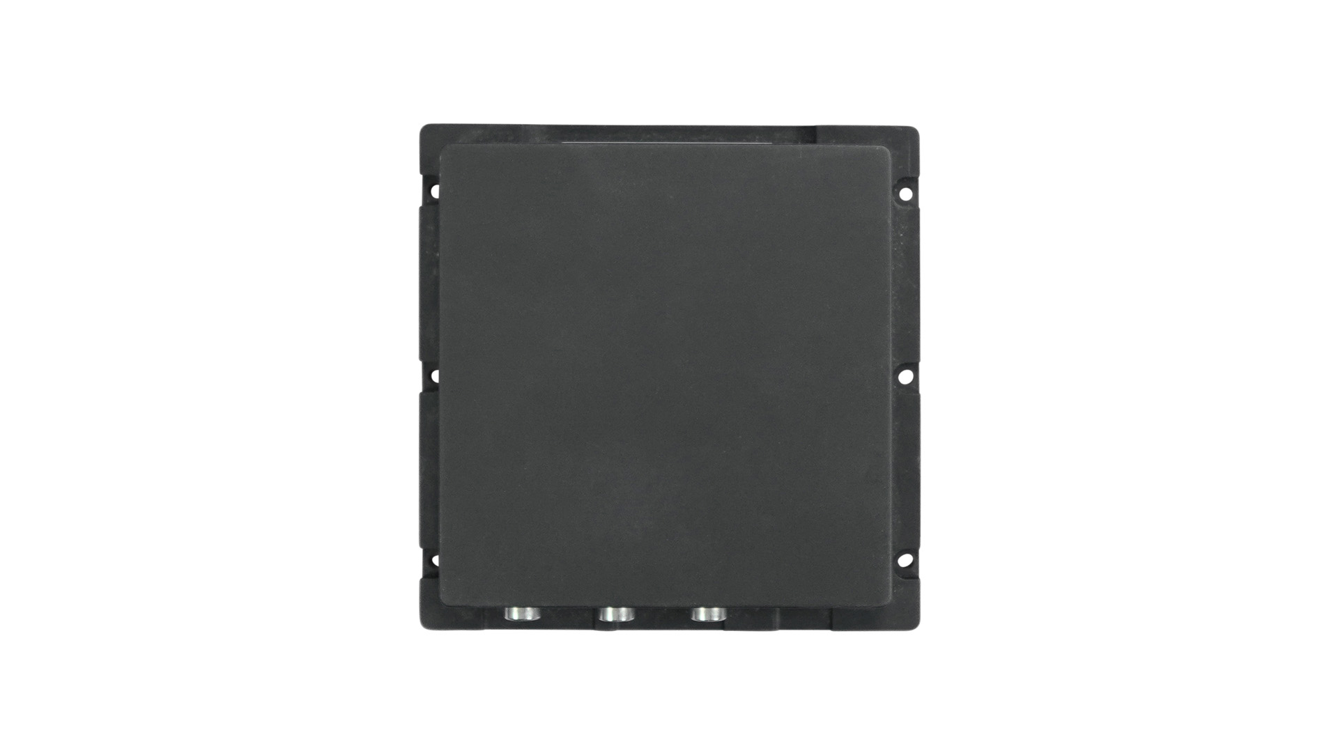


Eth-ReporterII
Rugged, Small, Lightweight, Ethernet, FPGA-Based Multi-Function I/O Controller
- User FPGA for applications requirements via RS-232/422/488 (encryption, custom communication protocols, etc.)
- One GigE port with ModBus TCP
- Up to three RS-232/422/485 ports via User FPGA
- Thirty six general purpose LVTTL lines with 1KΩ pull up resistor
- Twelve buffered general purpose LVTTL lines with 24mA drive per line
- Four low-side open drain output channels with 1A drive per channel
- Eight RS-422 output channels, twelve input channels
Share this product
LinkedIn
Eth-ReporterII
Rugged, Small, Lightweight, Ethernet, FPGA-Based Multi-Function I/O Controller
The Eth-ReporterII is an Ethernet-based Multi-Function I/O module that employs dual Altera Cyclone FPGAs for maximum deterministic performance and I/O capability. The module provides an Ethernet network interface for Digital I/O, Analog, and Serial communication. Although it is fully functional as delivered, the User FPGA can be modified for custom bus implementations, allowing maximum flexibility and pre-processing capability for time-sensitive applications. To communicate with the host, the ATC-ETH-DIG-I/O uses the simple standard networking protocol Modbus, which allows for control and data transfers.
The Eth-ReporterII uses a single 160 pin I/O connector for all system inputs and outputs. The I/O connector is a high density D-type connector with female pins. The mating cable end connector is available in a number of configurations to meet specific application requirements.
All Features:
- User FPGA for applications requirements via RS-232/422/488 (encryption, custom communication protocols, etc.)
- One GigE port with ModBus TCP
- Up to three RS-232/422/485 ports via User FPGA
- Thirty six general purpose LVTTL lines with 1KΩ pull up resistor
- Twelve buffered general purpose LVTTL lines with 24mA drive per line
- Four low-side open drain output channels with 1A drive per channel
- Eight RS-422 output channels, twelve input channels
- One I2C interface channel
- One SPI interface channel
- Eight 16-bit A/D channels for external voltage monitor
- Internal voltage monitor capability
- Designed and manufactured in USA
Environment:
- Operating temperature: -40° to +85° C
- Shock: 30G, 15ms sawtooth
- Vibration: 15G, 5-2000 Hz
- Input voltage: +12 to +28 VDC
Mechanical:
- Size: 5.4″ x 5.5″ x 1.6″ (WDH)
- Rear panel I/O: 160-pin Molex
- Weight: 1.67 lbs
- MTBF: >250,000 hours
- User FPGA for applications requirements via RS-232/422/488 (encryption, custom communication protocols, etc.)
- One GigE port with ModBus TCP
- Up to three RS-232/422/485 ports via User FPGA
- Thirty six general purpose LVTTL lines with 1KΩ pull up resistor
- Twelve buffered general purpose LVTTL lines with 24mA drive per line
- Four low-side open drain output channels with 1A drive per channel
- Eight RS-422 output channels, twelve input channels
| Mechanical Interface | Switched Mezzanine Card (XMC) Interface confirming to ANSI/VITA 42.0-2008 (Auxiliary Standard) Standard single-width (149mm x 74mm) | |||||||||
| Electrical Interface | PCI Express x4 Link (Base Specification 2.1) compliant interface conforming to ANSI/VITA 42.3-2006 (PCI Express Protocol Layer Standard) | |||||||||
| PCI Express Switch | PI7C9X2G312GP (Pericom) | |||||||||
| PCI Express to PCI Bridge | XIO2001 (Texas Instruments) | |||||||||
| User configurable FPGA | TXMC639-10R: XC7K160T-2FBG676I (AMD) TXMC639-11R: XC7K325T-2FBG676I (AMD) | |||||||||
| SPI-Flash | MT25QL128 (Micron) 128 Mbit (contains TXMC639 FPGA BRD) or compatible; +3.3 V supply voltage | |||||||||
| DDR3 RAM | 2x MT41K256M16TW-107 (Micron) 256Meg x 32 bit | |||||||||
| Board Configuration Controller | LCMXO2-7000HC (Lattice) | |||||||||
| ADC | LTC2320 -16 (Analog Devices) | |||||||||
| DAC | AD5547BRUZ (Analog Devices) | |||||||||
| A/D Channels | TXMC639-10R: 8 Differential 16bit A/D Channels TXMC639-11R: 16 Differential 16bit A/D Channels Input Configuration per BCC Device: Input Voltage Ranges: Differental : ±20.57 V, ±10.28 V or ±5.14 V (Single-Ended: ±10.28 V, ±5.14 V or ±2.57 V) All analog inputs are connected via an impedance converter and a second operation amplifier for level adjustment and filtering to the differential ADC inputs. The -3 dB limit of this input stage is at approx. 8MHz | |||||||||
| D/A Channels | TXMC639-10R: 4 Single-Ended 16 Bit D/A Channels TXMC639-11R: 8 Single-Ended 16 Bit D/A Channels Output range configurable per D/A channel. Maximum single-ended Output Voltage – Vout: ±10 V Maximum Output Drive Current for each Output: 10 mA Maximum Capacitive Load for each Output: 1000 pF Typical Settling Time for a 10 mA / 1000 pF: < 1 µs | |||||||||
| Digital Front I/O Channels | 32 digital I/O Lines
| |||||||||
| Digital Rear I/O Channels | 64 direct FPGA I/O lines to P14 Rear I/O connector
4 MGT line to P16 Rear I/O connector
| |||||||||
| Front I/O | Front I/O Samtec – ERF8_050_01_L_D_RA_L_TR | |||||||||
| P14 Rear I/O | 64 pin Mezzanine Connector (Molex 71436-2864 or compatible) | |||||||||
| P16 Rear I/O | 114 pin Mezzanine Connector (Samtec – ASP-105885-01) | |||||||||
| Power Requirements 1) | Depends on FPGA design With TXMC639 Board Reference Design / without external load
| |||||||||
| Temperature Range | Operating: – 40 °C to + 85 °C Storage: – 55 °C to + 125 °C | |||||||||
| MTBF 1) | 157 000 h to 161 000 h | |||||||||
| Humidity | 5% – 95% non-condensing | |||||||||
| Weight | 140 g |
1) depends on variant, for further details see User Manual
TXMC639-10R
| 8x Analog In, 4x Analog Out, XC7K160T-2FBG676 Kintex™ 7 FPGA AMD Kintex™ 7 FPGA (XC7K160T-2FBG676), 1GB DDR3, 8x Analog In, 4x Analog Out, 32x digital Front I/O, 64x direct FPGA Rear I/O Lines and 4x MGTs Rear I/O |
TXMC639-11R
| 16x Analog In, 8x Analog Out, XC7K325T-2FBG676 Kintex™ 7 FPGA AMD Kintex™ 7 FPGA (XC7K325T-2FBG676), 1GB DDR3, 16x Analog In, 8x Analog Out, 32x digital Front I/O, 64x direct FPGA Rear I/O Lines and 4x MGTs Rear I/O |
SOFTWARE
Share this product
LinkedIn

