- 8 Channels D/A
- 1 μS settling time, 0-5V range
- 16 Bits Resolution
- 2- or 4-quadrant, 6.8 MHz BW multiplying DAC
- ±1 LSB DNL ±1 LSB INL
- Low noise: 12 nV/√Hz
- Built-in 4-quadrant resistors allow 0 V to –10 V, 0 V to +10 V, or ±10 V outputs
- Selectable zero-scale/midscale power-on presets per channel
- Up to 30 mA Output Drive
- Front Panel 68-pin MDR Connector
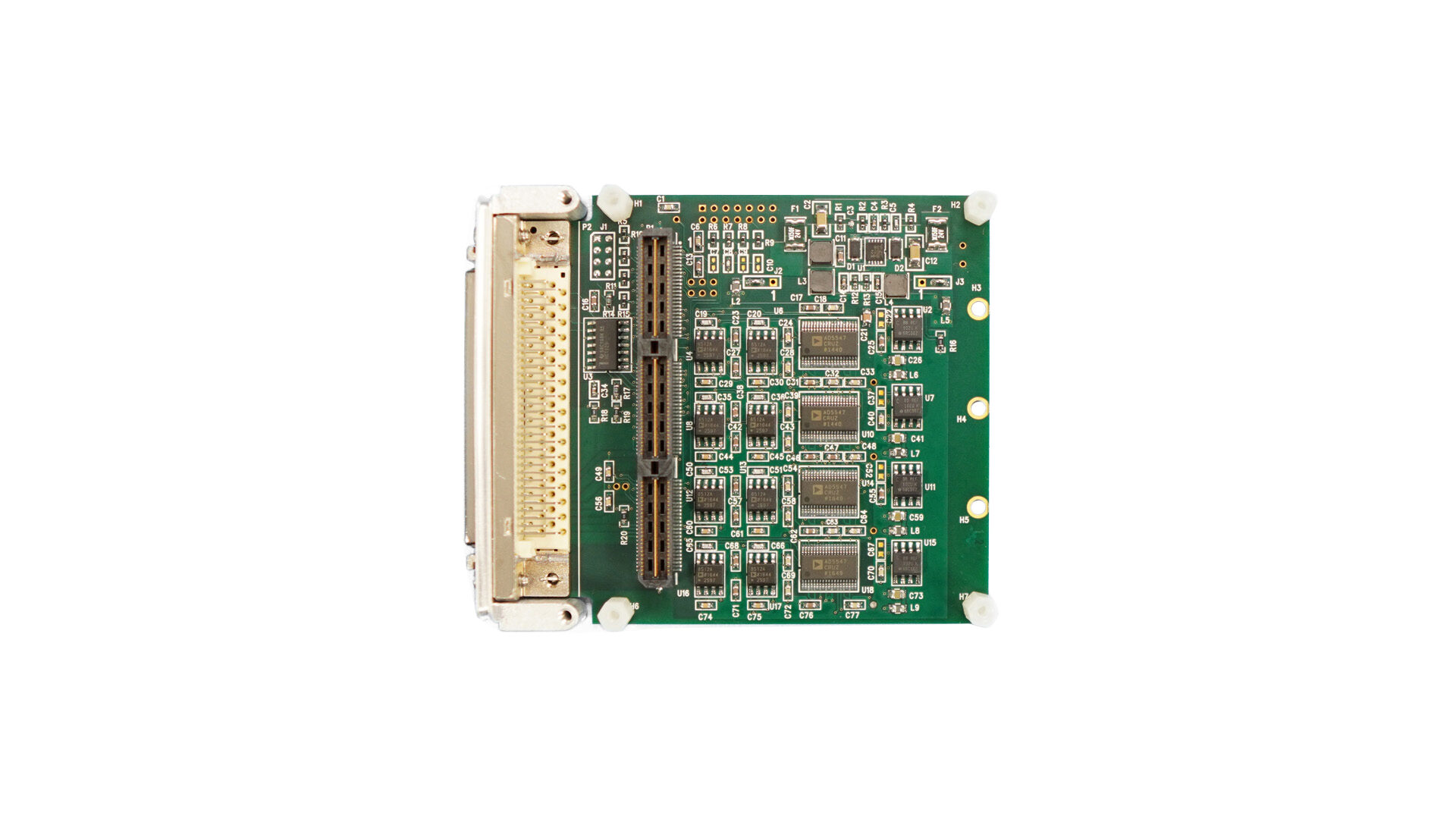


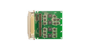
AXM-DA8-16
AXM FGA Interface 8 1μs D/A Channels
- 8 Channels D/A
- 1 μS settling time, 0-5V range
- 16 Bits Resolution
- 2- or 4-quadrant, 6.8 MHz BW multiplying DAC
- ±1 LSB DNL ±1 LSB INL
- Low noise: 12 nV/√Hz
- Built-in 4-quadrant resistors allow 0 V to –10 V, 0 V to +10 V, or ±10 V outputs
- Selectable zero-scale/midscale power-on presets per channel
- Up to 30 mA Output Drive
- Front Panel 68-pin MDR Connector
Share this product
LinkedIn
AXM-DA8-16
AXM FGA Interface 8 1μs D/A Channels
The AXM-DA8-16 is a sophisticated 8-channel, 16-bit Digital-to-Analog converter module, offering precise and high-speed signal generation. It is controlled via the AXM interface and features a 1 μs settling time with a default output range of 0-5V. The module supports both 2- and 4-quadrant operations, allowing for outputs from 0 V to ±10 V or other programmable ranges using built-in resistors. It boasts high accuracy with ±1 LSB DNL and INL, low noise of 12 nV/√Hz, and a bandwidth of 6.8 MHz, ensuring minimal signal distortion. Each channel can drive up to 30 mA, making it suitable for various loads. Additional features include selectable power-on presets for zero-scale or midscale output and a convenient 68-pin MDR front panel connector. This module, paired with the AXM interface, is well-suited for industrial control, instrumentation, and automated testing applications requiring reliable and flexible analog signal generation.
Part Number: AXM-DA8-16
Description: AXM 8 D/A 1 μs channels
Option: Add “C” for Conformal coat (e.g., AXM-DA8-16C)
Optional Accessories:
CBL-MDR68: 68 Pins MDR Cable, 1 meter length
Data Sheet – Link Here
- 8 Channels D/A
- 1 μS settling time, 0-5V range
- 16 Bits Resolution
- 2- or 4-quadrant, 6.8 MHz BW multiplying DAC
- ±1 LSB DNL ±1 LSB INL
- Low noise: 12 nV/√Hz
- Built-in 4-quadrant resistors allow 0 V to –10 V, 0 V to +10 V, or ±10 V outputs
- Selectable zero-scale/midscale power-on presets per channel
- Up to 30 mA Output Drive
- Front Panel 68-pin MDR Connector
| Mechanical Interface | Switched Mezzanine Card (XMC) Interface confirming to ANSI/VITA 42.0-2008 (Auxiliary Standard) Standard single-width (149mm x 74mm) | |||||||||
| Electrical Interface | PCI Express x4 Link (Base Specification 2.1) compliant interface conforming to ANSI/VITA 42.3-2006 (PCI Express Protocol Layer Standard) | |||||||||
| PCI Express Switch | PI7C9X2G312GP (Pericom) | |||||||||
| PCI Express to PCI Bridge | XIO2001 (Texas Instruments) | |||||||||
| User configurable FPGA | TXMC639-10R: XC7K160T-2FBG676I (AMD) TXMC639-11R: XC7K325T-2FBG676I (AMD) | |||||||||
| SPI-Flash | MT25QL128 (Micron) 128 Mbit (contains TXMC639 FPGA BRD) or compatible; +3.3 V supply voltage | |||||||||
| DDR3 RAM | 2x MT41K256M16TW-107 (Micron) 256Meg x 32 bit | |||||||||
| Board Configuration Controller | LCMXO2-7000HC (Lattice) | |||||||||
| ADC | LTC2320 -16 (Analog Devices) | |||||||||
| DAC | AD5547BRUZ (Analog Devices) | |||||||||
| A/D Channels | TXMC639-10R: 8 Differential 16bit A/D Channels TXMC639-11R: 16 Differential 16bit A/D Channels Input Configuration per BCC Device: Input Voltage Ranges: Differental : ±20.57 V, ±10.28 V or ±5.14 V (Single-Ended: ±10.28 V, ±5.14 V or ±2.57 V) All analog inputs are connected via an impedance converter and a second operation amplifier for level adjustment and filtering to the differential ADC inputs. The -3 dB limit of this input stage is at approx. 8MHz | |||||||||
| D/A Channels | TXMC639-10R: 4 Single-Ended 16 Bit D/A Channels TXMC639-11R: 8 Single-Ended 16 Bit D/A Channels Output range configurable per D/A channel. Maximum single-ended Output Voltage – Vout: ±10 V Maximum Output Drive Current for each Output: 10 mA Maximum Capacitive Load for each Output: 1000 pF Typical Settling Time for a 10 mA / 1000 pF: < 1 µs | |||||||||
| Digital Front I/O Channels | 32 digital I/O Lines
| |||||||||
| Digital Rear I/O Channels | 64 direct FPGA I/O lines to P14 Rear I/O connector
4 MGT line to P16 Rear I/O connector
| |||||||||
| Front I/O | Front I/O Samtec – ERF8_050_01_L_D_RA_L_TR | |||||||||
| P14 Rear I/O | 64 pin Mezzanine Connector (Molex 71436-2864 or compatible) | |||||||||
| P16 Rear I/O | 114 pin Mezzanine Connector (Samtec – ASP-105885-01) | |||||||||
| Power Requirements 1) | Depends on FPGA design With TXMC639 Board Reference Design / without external load
| |||||||||
| Temperature Range | Operating: – 40 °C to + 85 °C Storage: – 55 °C to + 125 °C | |||||||||
| MTBF 1) | 157 000 h to 161 000 h | |||||||||
| Humidity | 5% – 95% non-condensing | |||||||||
| Weight | 140 g |
1) depends on variant, for further details see User Manual
TXMC639-10R
| 8x Analog In, 4x Analog Out, XC7K160T-2FBG676 Kintex™ 7 FPGA AMD Kintex™ 7 FPGA (XC7K160T-2FBG676), 1GB DDR3, 8x Analog In, 4x Analog Out, 32x digital Front I/O, 64x direct FPGA Rear I/O Lines and 4x MGTs Rear I/O |
TXMC639-11R
| 16x Analog In, 8x Analog Out, XC7K325T-2FBG676 Kintex™ 7 FPGA AMD Kintex™ 7 FPGA (XC7K325T-2FBG676), 1GB DDR3, 16x Analog In, 8x Analog Out, 32x digital Front I/O, 64x direct FPGA Rear I/O Lines and 4x MGTs Rear I/O |
SOFTWARE
Share this product
LinkedIn