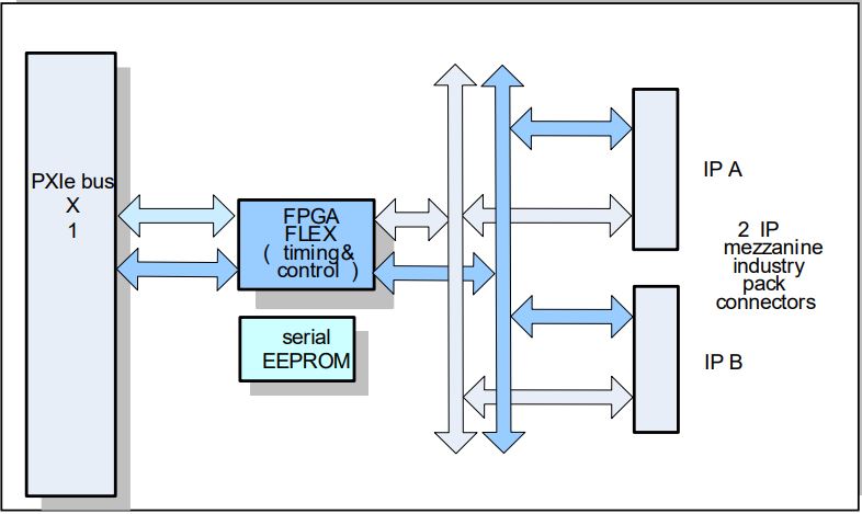
- Form Factor: 3U PXIe format, slave dual industry pack carrier
- Industry Pack Support: Supports up to two IP modules, single or double-wide form factor
- IP Operation Frequency: 8 MHz or 32 MHz per slot, software programmable
- Access Method: Direct I/O or memory-mapped access from PXIe bus via FPGA x1 PCIe
- Interrupt Support: Full interrupt support of host
- I/O Connectors: Front panel I/O connectors for all IPs; rear connector I/O also available
- Maximum I/Os: Up to 96 I/Os on one single slot
PXIe-SIP
PXIe Slave Dual Industry Pack Carrier
- Form Factor: 3U PXIe format, slave dual industry pack carrier
- Industry Pack Support: Supports up to two IP modules, single or double-wide form factor
- IP Operation Frequency: 8 MHz or 32 MHz per slot, software programmable
- Access Method: Direct I/O or memory-mapped access from PXIe bus via FPGA x1 PCIe
- Interrupt Support: Full interrupt support of host
- I/O Connectors: Front panel I/O connectors for all IPs; rear connector I/O also available
- Maximum I/Os: Up to 96 I/Os on one single slot
Share this product
LinkedIn
PXIe-SIP
PXIe Slave Dual Industry Pack Carrier
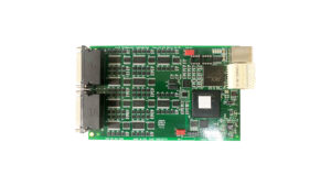
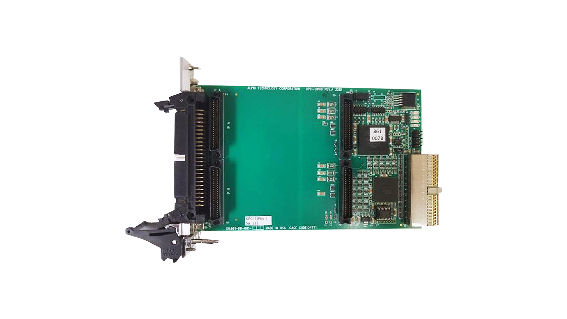
The PXIe-SIP is a 3U format slave module designed as a Compact PXIe bus IP carrier. It provides both mechanical support and electrical interfaces for accommodating either two single-width IP modules or one double-width IP module. This flexibility allows multiple PXIe-SIP boards to be installed within a single system, enhancing the scalability and modularity of the setup.
Industry Pack Specifications
- Meets ANSI/VITA 4-1995 standards.
- Supports 8/32 MHz synchronous operation.
- Supports ID, 128 byte I/O, interrupt, and 8 Mbyte memory spaces.
- Provides 2 interrupts per module.
- Two passive DMA channels are possible.
- Hardware self-timed per IP module, triggered via system reset and software control.
- Jumper or software time-out functions available.
- 5V and +/-12V resettable fuses per IP module.
- Supports 8/16-bit data on 3U boards and 32-bit data on 6U boards.
Operating Environment
- Operating Temperature:
- Commercial: 0 to +70 °C
- Optional: -40 °C to +85 °C
- Non-operating Temperature: -55 °C to +100 °C
- Airflow Requirement: 5 CFM
- Humidity: 5 to 90% (non-condensing)
- Altitude: Up to 10,000 feet
Mechanical Environment
- Size: 3U CPCI module, 100mm x 160mm
- Power Consumption: 1 watt
- Vibration Resistance: 0.5G, 20-2000 Hz random
- Shock Resistance: 20G, 11 ms, ½ sine
- Weight: 5 ounces
- MTBF: >250,000 hours
PCIe Bus Controller Features
- PICMG 1.1 standards compliance
- Zero wait state burst operation, with PCI bus bursts to 264 MB/sec and local bus bursts to 264 MB/sec
- 2 DMA channels
- Direct master and slave data transfers
- PCI bus INTA# interrupt, up to 2 interrupts from each IP
Ordering Information:
- Part Number: PXIe-SIP
- 3U PXIe Slave Industry Pack Carrier with Front I/O only
- Part Number: PXIe-SIP-I
- Same as above but with Industrial temperature rating: -40 °C to +85 °C
Optional Accessories:
- Part Number: CBL-68-VHDCI-L
- Cable, 68 Pins VHDCI-68, L = Length
- Part Number: TB-68-VHDCI
- Terminal block, 68 Pins VHDCI
- Form Factor: 3U PXIe format, slave dual industry pack carrier
- Industry Pack Support: Supports up to two IP modules, single or double-wide form factor
- IP Operation Frequency: 8 MHz or 32 MHz per slot, software programmable
- Access Method: Direct I/O or memory-mapped access from PXIe bus via FPGA x1 PCIe
- Interrupt Support: Full interrupt support of host
- I/O Connectors: Front panel I/O connectors for all IPs; rear connector I/O also available
- Maximum I/Os: Up to 96 I/Os on one single slot
| Mechanical Interface | Switched Mezzanine Card (XMC) Interface confirming to ANSI/VITA 42.0-2008 (Auxiliary Standard) Standard single-width (149mm x 74mm) | |||||||||
| Electrical Interface | PCI Express x4 Link (Base Specification 2.1) compliant interface conforming to ANSI/VITA 42.3-2006 (PCI Express Protocol Layer Standard) | |||||||||
| PCI Express Switch | PI7C9X2G312GP (Pericom) | |||||||||
| PCI Express to PCI Bridge | XIO2001 (Texas Instruments) | |||||||||
| User configurable FPGA | TXMC639-10R: XC7K160T-2FBG676I (AMD) TXMC639-11R: XC7K325T-2FBG676I (AMD) | |||||||||
| SPI-Flash | MT25QL128 (Micron) 128 Mbit (contains TXMC639 FPGA BRD) or compatible; +3.3 V supply voltage | |||||||||
| DDR3 RAM | 2x MT41K256M16TW-107 (Micron) 256Meg x 32 bit | |||||||||
| Board Configuration Controller | LCMXO2-7000HC (Lattice) | |||||||||
| ADC | LTC2320 -16 (Analog Devices) | |||||||||
| DAC | AD5547BRUZ (Analog Devices) | |||||||||
| A/D Channels | TXMC639-10R: 8 Differential 16bit A/D Channels TXMC639-11R: 16 Differential 16bit A/D Channels Input Configuration per BCC Device: Input Voltage Ranges: Differental : ±20.57 V, ±10.28 V or ±5.14 V (Single-Ended: ±10.28 V, ±5.14 V or ±2.57 V) All analog inputs are connected via an impedance converter and a second operation amplifier for level adjustment and filtering to the differential ADC inputs. The -3 dB limit of this input stage is at approx. 8MHz | |||||||||
| D/A Channels | TXMC639-10R: 4 Single-Ended 16 Bit D/A Channels TXMC639-11R: 8 Single-Ended 16 Bit D/A Channels Output range configurable per D/A channel. Maximum single-ended Output Voltage – Vout: ±10 V Maximum Output Drive Current for each Output: 10 mA Maximum Capacitive Load for each Output: 1000 pF Typical Settling Time for a 10 mA / 1000 pF: < 1 µs | |||||||||
| Digital Front I/O Channels | 32 digital I/O Lines
| |||||||||
| Digital Rear I/O Channels | 64 direct FPGA I/O lines to P14 Rear I/O connector
4 MGT line to P16 Rear I/O connector
| |||||||||
| Front I/O | Front I/O Samtec – ERF8_050_01_L_D_RA_L_TR | |||||||||
| P14 Rear I/O | 64 pin Mezzanine Connector (Molex 71436-2864 or compatible) | |||||||||
| P16 Rear I/O | 114 pin Mezzanine Connector (Samtec – ASP-105885-01) | |||||||||
| Power Requirements 1) | Depends on FPGA design With TXMC639 Board Reference Design / without external load
| |||||||||
| Temperature Range | Operating: – 40 °C to + 85 °C Storage: – 55 °C to + 125 °C | |||||||||
| MTBF 1) | 157 000 h to 161 000 h | |||||||||
| Humidity | 5% – 95% non-condensing | |||||||||
| Weight | 140 g |
1) depends on variant, for further details see User Manual
TXMC639-10R
| 8x Analog In, 4x Analog Out, XC7K160T-2FBG676 Kintex™ 7 FPGA AMD Kintex™ 7 FPGA (XC7K160T-2FBG676), 1GB DDR3, 8x Analog In, 4x Analog Out, 32x digital Front I/O, 64x direct FPGA Rear I/O Lines and 4x MGTs Rear I/O |
TXMC639-11R
| 16x Analog In, 8x Analog Out, XC7K325T-2FBG676 Kintex™ 7 FPGA AMD Kintex™ 7 FPGA (XC7K325T-2FBG676), 1GB DDR3, 16x Analog In, 8x Analog Out, 32x digital Front I/O, 64x direct FPGA Rear I/O Lines and 4x MGTs Rear I/O |
SOFTWARE
Share this product
LinkedIn